All Questions
What Are The Key Advantages Of Pecvd Compared To Lpcvd? Lower Temperatures, Faster Deposition, And More
Explore PECVD's low-temperature processing, high deposition rates, and film control for semiconductor and temperature-sensitive applications.
What Were The Initial Configurations Of Plasma Enhanced Chemical Vapor Deposition (Pecvd) Systems? Explore Early Semiconductor Innovations
Discover the initial PECVD system configurations adapted from LPCVD, their limitations, and evolution to modern cold-wall reactors for superior film deposition.
How Does Pecvd Contribute To The Performance Of New Energy Vehicle Systems? Enhance Reliability And Safety
Discover how PECVD technology provides superior protection for NEV electronics, boosting stability, lifespan, and safety in harsh conditions.
What Specific Thin Films Are Commonly Deposited Using Pecvd In Integrated Circuits? Essential Dielectrics For Ics
Learn about PECVD-deposited silicon dioxide and silicon nitride thin films for insulation and protection in integrated circuits, with low-temperature benefits.
How Does Pecvd Compare To Traditional Cvd In Semiconductor Processes? Discover Key Differences For Better Thin-Film Deposition
Compare PECVD and traditional CVD for semiconductor processes: learn about energy sources, temperature requirements, and advantages like low-temperature deposition on sensitive substrates.
What Advantages Do Pecvd Polymer Nanofilms Offer In Semiconductor Applications? Discover Enhanced Protection And Reliability
Explore PECVD polymer nanofilms' benefits: low-temperature deposition, high purity, and robust protection for semiconductor reliability and performance.
What Role Does Pecvd Play In Creating Optical Coatings? Achieve Precision Thin Films For Enhanced Optics
Discover how PECVD enables low-temperature deposition of anti-reflective, protective, and tailored optical coatings with precise refractive index control.
How Does Pecvd Technology Benefit Solar Cell Production? Boost Efficiency And Cut Costs With Advanced Thin Films
Discover how PECVD technology enhances solar cell efficiency through anti-reflection coatings and surface passivation, while enabling low-temperature, high-throughput manufacturing.
What Are The Main Applications Of Pecvd In Semiconductor Manufacturing? Essential For Low-Temperature Dielectric Films
Explore PECVD's key roles in depositing SiO₂, Si₃N₄, and low-k dielectrics for isolation, passivation, and high-performance chips at low temperatures.
What Makes Pecvd A Cornerstone Technology In Modern Fabrication Processes? Achieve Low-Temperature, High-Quality Film Deposition
Discover how PECVD enables high-quality thin film deposition on heat-sensitive substrates for electronics, optics, and solar cells with low-temperature plasma processes.
How Does Pecvd Compare To Lpcvd? Choose The Right Cvd Method For Your Lab
Compare PECVD and LPCVD: temperature, speed, and film quality differences for semiconductor and material science applications.
How Does Pecvd Compare To Traditional Cvd? Unlock Low-Temperature Deposition For Sensitive Substrates
Explore PECVD vs. CVD: key differences in energy sources, temperature ranges, and applications for precise film deposition on heat-sensitive materials.
What Are Some Common Applications Of Pecvd? Unlock Versatile Thin-Film Solutions For Your Lab
Explore PECVD applications in semiconductors, optics, and barrier coatings for low-temperature, high-performance thin films in various industries.
What Are The Advantages Of Using Pecvd For Thin-Film Deposition? Unlock Low-Temp, High-Quality Films
Discover PECVD advantages: low-temperature operation, tunable film properties, and high efficiency for electronics, optics, and MEMS applications.
What Happens During The Chemical Reactions And Deposition Phase Of Pecvd? Master Low-Temperature Thin Film Deposition
Explore the PECVD deposition phase: adsorption, reaction, and desorption steps for high-quality thin films at low temperatures, with key process controls.
How Is Plasma Generated In The Pecvd Process? Unlock Low-Temperature Thin-Film Deposition
Learn how plasma is generated in PECVD using electric fields in low-pressure gases for efficient, low-temperature thin-film deposition on various substrates.
How Does Pecvd Begin The Deposition Process? Unlock Low-Temperature Thin Film Deposition
Learn how PECVD starts with plasma generation for low-temperature thin film deposition on sensitive substrates, enhancing material engineering.
What Are The Opportunities And Challenges Of Pecvd For Future Applications Of 2D Materials? Unlock Scalable Growth For Flexible Electronics
Explore PECVD's role in 2D materials: low-temperature, transfer-free growth for flexible electronics and sensors, with insights on scalability and quality control.
What Are Some Promising Applications Of Pecvd-Prepared 2D Materials? Unlock Advanced Sensing And Optoelectronics
Explore PECVD applications in 2D materials for sensors, optoelectronics, and human-machine interfaces, enabling low-temperature, direct device integration.
How Do The Clean Surfaces And Interfaces Of Pecvd-Prepared Materials Benefit Their Applications? Boost Performance In Electronics
Discover how PECVD's clean interfaces enhance carrier mobility, thermal dissipation, and power handling in advanced devices like graphene FETs.
What Are The Advantages Of Pecvd For Preparing 2D Materials? Unlock Scalable, Low-Temp Fabrication
Discover how PECVD enables low-temperature, transfer-free deposition of 2D materials for flexible electronics and industrial-scale production.
What Types Of 2D Materials Can Be Prepared Using Pecvd? Discover Versatile Synthesis For Advanced Electronics
Explore PECVD for synthesizing graphene, h-BN, and ternary 2D materials with low-temperature, transfer-free growth, ideal for scalable industrial applications.
How Does The Competition Between Etching, Nucleation, And Deposition In Pecvd Affect Material Preparation? Master Precise Control For Tailored Materials
Explore how balancing etching, nucleation, and deposition in PECVD enables tailored material morphologies, from films to nanostructures, for advanced applications.
What Is Plasma-Enhanced Chemical Vapor Deposition (Pecvd), And Why Is It Desirable? Discover Low-Temperature Thin Film Solutions
Learn about PECVD's low-temperature process for high-quality thin films on heat-sensitive substrates, enabling advanced electronics and material fabrication.
What Are Decorative Coatings, And How Does Pecvd Enhance Them? Unlock Durable, High-Performance Surfaces
Learn how PECVD decorative coatings add vibrant colors with superior scratch resistance and optical control for enhanced durability and aesthetics.
How Is Pecvd Used To Deposit Hard Coatings? Achieve Durable, Low-Temperature Surface Protection
Learn how PECVD deposits hard coatings like silicon nitride at low temperatures for wear resistance on sensitive materials, enhancing durability and performance.
What Are Gas Barrier Films, And How Is Pecvd Involved In Their Creation? Discover Advanced Packaging Solutions
Learn how PECVD creates gas barrier films to prevent oxygen and moisture permeation, enhancing shelf life for sensitive products like food and electronics.
How Is Pecvd Applied In Biomedical Research? Unlock Advanced Surface Engineering For Medical Devices
Discover how PECVD enables low-temperature, biocompatible coatings for implants, biosensors, and drug delivery systems in biomedical research.
What Are Barrier Coatings, And How Is Pecvd Used In Their Deposition? Discover Low-Temp, High-Performance Solutions
Learn how PECVD barrier coatings protect sensitive materials with low-temperature, dense, and conformal films for enhanced product durability and reliability.
How Does Pecvd Contribute To Microelectronics And Mems Devices? Enable Low-Temperature Thin Film Deposition
Learn how PECVD enables low-temperature deposition of insulating and protective films for microelectronics and MEMS, preventing thermal damage in sensitive devices.
What Is The Significance Of Pecvd In Flat Panel Display Manufacturing? Enabling High-Performance, Low-Temperature Deposition
Discover how PECVD enables low-temperature thin-film deposition for TFTs and OLEDs in flat panel displays, ensuring performance and longevity.
How Is Pecvd Applied In Optical Coatings? Enhance Light Control With Precision Films
Explore PECVD's role in optical coatings for anti-reflective layers, mirrors, and protective films, enabling precise refractive index tuning and low-temperature processing.
What Role Does Pecvd Play In Solar Cell Production? Boost Efficiency With Advanced Thin-Film Deposition
Discover how Plasma Enhanced Chemical Vapor Deposition (PECVD) enhances solar cell efficiency through anti-reflective coatings and precise thin-film deposition for scalable manufacturing.
How Is Pecvd Utilized In Semiconductor Manufacturing? Essential For Low-Temperature Thin-Film Deposition
Explore how PECVD enables low-temperature deposition of dielectric films in semiconductor manufacturing, protecting heat-sensitive components and enhancing device performance.
What Are The Primary Applications Of Plasma-Enhanced Chemical Vapor Deposition (Pecvd) Systems? Unlock Low-Temperature Thin Film Deposition
Explore PECVD applications in semiconductors, solar cells, and optical coatings. Learn how low-temperature plasma enables thin film deposition on sensitive substrates.
What Is Inductively Coupled Plasma Chemical Vapor Deposition (Icp-Cvd)? Achieve Superior Low-Temperature Thin Films
Learn how ICP-CVD enables high-quality, dense thin film deposition at low temperatures, ideal for heat-sensitive materials in semiconductors and MEMS.
What Are The Advantages Of Plasma-Enhanced Deposition? Achieve Low-Temperature, High-Quality Thin Films
Discover how PECVD enables low-temperature thin film deposition with superior control and high rates, ideal for sensitive substrates and efficient manufacturing.
What Are The Typical Conditions For Plasma-Enhanced Cvd Processes? Achieve Low-Temperature Thin Film Deposition
Explore PECVD's low-pressure, low-temperature conditions (50-400°C) for depositing thin films on heat-sensitive substrates without damage.
What Are The Key Steps In The Pecvd Mechanism? Master Low-Temperature Thin Film Deposition
Learn the 5 essential steps of PECVD for low-temperature thin film deposition, ideal for electronics and sensitive materials. Enhance your process efficiency.
What Are The Main Technologies For Thin Film Deposition? Choose Pvd, Cvd, Or Pecvd For Your Needs
Explore PVD, CVD, and PECVD thin film deposition technologies: their mechanisms, advantages, and ideal applications for precise material coating.
How Does Rf Power Affect The Quality And Deposition Rate Of The Film In Pecvd? Optimize Your Process For Superior Films
Learn how RF power controls deposition rate and film quality in PECVD, including trade-offs, frequency effects, and optimization strategies for better results.
What Is The Typical Setup For Pecvd In Terms Of Chamber And Electrode Configuration? Optimize Thin Film Deposition
Learn about PECVD chamber and electrode setups, including parallel-plate reactors, showerhead electrodes, and low-temperature processing for uniform thin films.
How Does The Reaction Gas Transform Into A Solid Film In Pecvd? Master Plasma-Driven Thin Film Deposition
Learn the step-by-step PECVD process where plasma energizes gases to form solid films at low temperatures, ideal for sensitive substrates.
What Is The Process Of Glow Discharge In Pecvd? Unlock Low-Temperature Thin Film Deposition
Explore how glow discharge in PECVD enables low-temperature thin film deposition on sensitive substrates, enhancing efficiency and versatility in labs.
How Does Pecvd Compare To Traditional Cvd Equipment In Terms Of Film Formation? Discover The Key Differences For Your Lab
Explore PECVD vs. traditional CVD: lower temperatures, faster deposition, and film quality. Ideal for semiconductor and sensitive device fabrication.
What Role Does The Rf Power Supply Play In Pecvd Thin Film Deposition? Master Plasma Control For Superior Films
Learn how RF power supply drives PECVD thin film deposition, controlling plasma, deposition rate, film density, stress, and uniformity for optimal results.
What Does Pecvd Stand For And What Is Its Primary Function? Discover Low-Temperature Thin Film Deposition
Learn about Plasma-Enhanced Chemical Vapor Deposition (PECVD), its low-temperature process, advantages, and applications for uniform thin films on sensitive substrates.
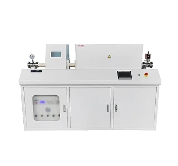
What Are The System Specifications Of The Pecvd System? Unlock Precision Thin-Film Deposition
Explore PECVD system specs: RF/LF power, vacuum performance, gas control, and thermal management for superior thin-film deposition in R&D and production.
What Are Some Key Features Of The Pecvd System? Unlock Low-Temp, High-Rate Thin Film Deposition
Explore PECVD system features like plasma-enhanced deposition, low-temperature processing, high deposition rates, and uniform film quality for advanced materials.
What Gases Are Used In The Pecvd System? Optimize Thin Film Deposition With Precise Gas Selection
Learn about key PECVD gases like silane, ammonia, and argon for silicon-based films, process control, and chamber cleaning to enhance deposition quality.
What Materials Are Allowed In The Pecvd System? Ensure Compatibility For Superior Thin-Film Deposition
Learn which substrates and films are compatible with PECVD systems, including silicon, quartz, and common dielectrics, to optimize your lab processes.
What Wafer Sizes Does The Pecvd System Support? Find The Perfect Fit For Your Substrates
Learn about PECVD system substrate compatibility, including round wafers up to 6 inches and square formats, for semiconductor, solar, and optics applications.
What Is The Temperature Range Of The Pecvd System's Variable Temperature Stage? Unlock Versatile Film Deposition
Explore the PECVD system's variable temperature stage range from RT to 600°C for precise control over film quality, stress, and deposition rates.
What Are The Main Techniques Supported By The Pecvd System? Discover Low-Temperature Thin Film Deposition
Learn about PECVD techniques for depositing amorphous silicon, silicon dioxide, and silicon nitride films at low temperatures for enhanced device fabrication.
What Are The Key Advantages Of The Pecvd Process? Unlock Low-Temp, High-Speed Film Deposition
Discover PECVD's benefits: lower temperatures, faster deposition, superior film quality, and versatility for heat-sensitive materials and high-throughput manufacturing.
What Are Some Alternative Power Sources Used In Pecvd Reactors Besides Rf? Explore Dc And Microwave Options
Learn about DC and microwave power sources in PECVD reactors, their mechanisms, substrate compatibility, and impact on film quality for better process selection.
What Is The Role Of Rf Power In Pecvd And How Does The Rf-Pecvd Process Work? Master Thin Film Deposition Control
Learn how RF power in PECVD creates plasma for low-temperature thin film growth, controlling deposition rate, film stress, and step coverage.
How Are Pecvd Reactors Classified And What Are The Main Differences Between Direct And Remote Pecvd Systems? Discover The Best Fit For Your Lab
Learn how PECVD reactors are classified into direct and remote systems, their key differences in plasma proximity, film quality, and applications for optimal lab performance.
What Types Of Materials Can Be Deposited Using Pecvd And On Which Substrates? Unlock Versatile Thin-Film Solutions
Explore PECVD material deposition: dielectrics, semiconductors, protective coatings on silicon, metals, plastics. Low-temperature process for diverse substrates.
What Is Plasma Enhanced Chemical Vapor Deposition (Pecvd) And How Does It Differ From Conventional Cvd? Unlock Low-Temperature Thin Film Deposition
Explore PECVD vs. CVD: Learn how plasma enables low-temperature thin film deposition on heat-sensitive materials, with key differences in energy source and applications.
How Does Pecvd Achieve High-Quality Thin Films Without High Temperatures? Unlock Low-Temp, High-Quality Deposition
Learn how PECVD uses plasma for low-temperature thin film deposition, ideal for sensitive substrates. Explore process parameters and benefits.
What Safety Benefits Are Associated With The Lower Operating Temperature Of Pecvd? Enhance Lab Safety And Material Integrity
Discover how PECVD's low-temperature plasma process reduces thermal hazards, protects heat-sensitive materials, and improves operational safety in thin-film deposition.
How Does The Lower Temperature Of Pecvd Benefit Flexible And Organic Electronics? Unlock Gentle, High-Quality Film Deposition
Discover how PECVD's low-temperature process protects heat-sensitive substrates, reduces stress, and enables durable, high-performance flexible electronics.
Why Does Lpcvd Require Higher Temperatures Compared To Pecvd? Uncover The Energy Source Differences
Explore why LPCVD needs high heat while PECVD uses plasma for lower temps, impacting film quality, substrate compatibility, and throughput.
What Is The Key Advantage Of Pecvd Operating At Lower Temperatures? Enable Coating Of Heat-Sensitive Materials
Discover how PECVD's low-temperature process protects substrates, reduces defects, and enhances device integrity for advanced manufacturing.
How Does The Temperature Range Of Pecvd Compare To Lpcvd? Lower Heat For Better Device Protection
PECVD operates at 200-400°C vs LPCVD's 425-900°C, enabling low-temperature deposition for sensitive substrates and faster manufacturing.
What Is The Typical Temperature Range For Pecvd? Unlock Low-Temp Thin Film Deposition
Discover PECVD's 200-400°C range for depositing high-quality thin films on heat-sensitive substrates like semiconductors and plastics.
What Is The Advantage Of Plasma Cleaning In Pecvd Systems? Boost Yield With Automated In-Situ Cleaning
Discover how plasma cleaning in PECVD systems enhances uptime, repeatability, and yield by automating chamber maintenance for reliable thin-film deposition.
How Does Pecvd Control Film Properties? Master Thin-Film Engineering With Precision Control
Learn how PECVD adjusts gas flow, RF power, and temperature to tailor film properties like density, stress, and uniformity for various applications.
What Are Some Applications Of Pecvd? Unlock Low-Temperature Thin Film Solutions
Explore PECVD applications in semiconductors, solar cells, and coatings. Learn how low-temperature deposition enables advanced manufacturing on heat-sensitive materials.
What Are The Hardware Specifications For Pecvd Systems? Key Components For Precise Thin Film Deposition
Explore PECVD system hardware specs: electrode sizes up to 460mm, temperature control to 1200°C, and gas lines with MFCs for uniform film deposition.
What Types Of Films Can Be Deposited Using Pecvd? Explore Versatile Thin Films For Your Applications
Discover PECVD films like SiO₂, Si₃N₄, a-Si:H, DLC, and SiC for electronics, optics, and coatings at low temperatures.
What Are The Key Benefits Of Pecvd Systems? Achieve Low-Temperature, High-Quality Film Deposition
Discover PECVD system benefits: low-temperature operation, superior film quality, high deposition rates, and versatility for heat-sensitive substrates.
What Is Plasma Enhanced Chemical Vapour Deposition (Pecvd) Used For? Enable Low-Temperature, High-Quality Film Deposition
Discover PECVD uses for low-temperature deposition of thin films in semiconductors, solar cells, and coatings, enhancing device performance without heat damage.
Why Is Pecvd Suitable For Coating Temperature-Sensitive Materials? Enable Low-Temp, High-Quality Film Deposition
Discover how PECVD's low-temperature plasma process safely coats plastics and polymers, preventing damage while ensuring effective thin-film deposition.
What Types Of Properties Can Films Deposited By Pecvd Exhibit? Discover Versatile Coatings For Your Applications
Explore PECVD film properties like chemical resistance, optical tunability, and durability for microelectronics, coatings, and optics applications.
What Are The Limitations Of Pecvd? Overcome Process Control And Cost Challenges
Explore PECVD limitations like high sensitivity to parameters, contamination risks, and equipment costs. Learn how to optimize for low-temperature thin film deposition.
What Are Some Key Features And Benefits Of Pecvd? Unlock Low-Temperature Thin Film Deposition
Discover PECVD's low-temperature deposition, superior film quality, and versatility for electronics, optics, and medical devices.
What Are The Typical Operating Conditions For Pecvd? Optimize Your Film Deposition Process
Learn key PECVD operating conditions like temperature, pressure, and RF power for high-quality film deposition in semiconductors and coatings.
How Can Film Properties Be Tuned In Pecvd? Master Key Parameters For Optimal Film Control
Learn how to adjust gas flow, plasma power, and temperature in PECVD to tune film properties like refractive index, stress, and density for your applications.
What Are Some Common Applications Of Pecvd Films? Essential For Semiconductors, Solar Cells, And More
Explore PECVD film uses in microelectronics, MEMS, and coatings for enhanced insulation, protection, and optical properties in advanced manufacturing.
What Are The Advantages Of Pecvd In Film Deposition? Achieve Low-Temp, High-Quality Coatings
Discover PECVD benefits: low-temperature operation, uniform films, high deposition rates, and precise control for temperature-sensitive substrates and high-throughput manufacturing.
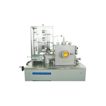
How Is A Pecvd System Configured? Optimize Low-Temperature Film Deposition For Your Lab
Learn how PECVD systems are configured with vacuum chambers, gas delivery, plasma generation, and control modules for precise, low-temperature film deposition.
What Is The Significance Of Pecvd In Modern Device Fabrication? Enable Low-Temperature Thin-Film Deposition
Discover how PECVD enables low-temperature thin-film deposition for microelectronics, biomedical devices, and optics, overcoming thermal limitations in fabrication.
Why Is Pecvd Suitable For Large-Scale Manufacturing? Unlock High-Yield, Low-Temp Film Deposition
Discover how PECVD enables large-scale manufacturing with low-temperature processing, high uniformity, and versatility for electronics and displays.
What Reactive Species Are Involved In The Pecvd Process? Unlock Low-Temperature Thin Film Deposition
Explore the key reactive species in PECVD—ions, electrons, radicals, and more—that enable efficient thin film deposition at lower temperatures for sensitive substrates.
What Factors Contribute To The Efficiency Of Pecvd? Boost Thin-Film Deposition With Low-Temp Plasma
Learn how plasma density, pressure, temperature, and system design optimize PECVD efficiency for faster, cost-effective thin-film deposition.
How Does Pecvd Differ From Heat-Activated Cvd? Unlock Low-Temperature Thin-Film Deposition
Explore key differences between PECVD and thermal CVD, including temperature, substrate compatibility, and film quality for advanced lab applications.
What Types Of Coatings Are Applied Using Pecvd In Mechanical Engineering? Enhance Wear And Corrosion Resistance
Explore PECVD coatings like DLC and oxides for superior wear and corrosion protection in mechanical engineering applications.
In Which Industries Is Pecvd Commonly Used? Essential For Semiconductors, Optics, And Solar Energy
Discover PECVD applications in semiconductors, optics, solar energy, and more for low-temperature thin film deposition on heat-sensitive materials.
What Are The Key Advantages Of Plasma-Enhanced Chemical Vapor Deposition (Pecvd)? Unlock Low-Temp, High-Quality Thin Films
Discover PECVD's key advantages: low-temperature processing, superior film quality, and versatility for semiconductors and optics. Enhance your manufacturing efficiency.
Why Is Pecvd Preferred For Thermally Sensitive Substrates? Enable Low-Temperature, High-Quality Thin Film Deposition
Discover how PECVD's plasma energy enables thin film deposition at 100-400°C, protecting sensitive substrates from heat damage while ensuring excellent film properties.
What Are The Advantages Of Pecvd Over Thermally Activated Cvd? Lower Temp, Higher Performance For Sensitive Substrates
Discover how PECVD's low-temperature plasma process enables coating of heat-sensitive materials, reduces defects, and boosts deposition rates vs. thermal CVD.
What Are Some Applications Of Pecvd Systems? Discover Versatile Thin-Film Solutions For Your Industry
Explore PECVD system applications in microelectronics, optics, packaging, and more. Learn how low-temperature deposition enhances heat-sensitive materials and complex shapes.
What Are The Primary Applications Of Pecvd-Deposited Films In The Semiconductor Industry? Essential For Electrical Isolation, Passivation, And Encapsulation
Explore how PECVD-deposited films enable electrical isolation, passivation, and encapsulation in semiconductors, ensuring device performance and reliability with low-temperature processing.
What Types Of Films Are Typically Deposited Using Pecvd? Discover Versatile Thin Films For Your Applications
Explore PECVD-deposited films like SiO₂, Si₃N₄, a-Si, and DLC for low-temperature, high-quality coatings in electronics and optics.
What Are The Main Advantages Of Using Pecvd Technology For Thin Film Deposition? Unlock Low-Temp, High-Quality Films
Discover PECVD's key benefits: low-temperature processing, superior film quality, precise control, and high deposition rates for advanced thin films.
What Are The Key Features Of Pecvd Equipment That Contribute To Film Uniformity? Enhance Your Deposition Precision
Learn how PECVD equipment features like uniform gas distribution, precise temperature control, and stable plasma ensure consistent film uniformity for better results.
Why Are Pecvd Systems Highly Regarded In The Semiconductor Industry? Unlock Low-Temperature, High-Quality Thin Films
Discover why PECVD systems are essential in semiconductors for low-temperature, precise thin-film deposition, enabling advanced device fabrication and reliability.
What Happens To The Reactive Species In The Pecvd Process After They Are Created? Uncover Their Journey To Film Formation
Learn how reactive species in PECVD diffuse, adsorb, and react on surfaces to build thin films, with insights on controlling film properties for better results.