In short, PECVD is unlocking a new generation of devices by enabling the practical fabrication of 2D materials for applications in advanced sensing, optoelectronics, and human-machine interfaces. Prototypical devices already include distributed pressure sensor arrays, electronic skins, and biochemical sensors, demonstrating a clear path toward commercial viability.
The true potential of PECVD isn't just in creating novel 2D materials, but in its ability to integrate them directly onto functional devices at low temperatures. This overcomes a critical manufacturing barrier, making complex applications like flexible sensors and integrated electronics commercially feasible.
Why PECVD is a Breakthrough for 2D Material Fabrication
Traditional methods for creating high-quality 2D materials often involve high temperatures and a complex transfer process, limiting their practical use. Plasma-Enhanced Chemical Vapor Deposition (PECVD) directly addresses these core limitations.
The Low-Temperature Advantage
The most significant benefit of PECVD is its ability to operate at much lower temperatures than conventional Chemical Vapor Deposition (CVD).
This allows for the direct growth of 2D materials on a wide variety of substrates, including flexible plastics and silicon wafers with pre-existing integrated circuits, without causing thermal damage.
Eliminating the Transfer Step
Traditional CVD grows 2D materials like graphene on a separate catalytic metal foil, which must then be chemically etched and transferred to the final device substrate.
This transfer process is a major source of defects, contamination, and cost. PECVD's ability to grow materials directly where they are needed results in cleaner surfaces and interfaces, which is critical for high-performance electronics.
Versatility in Material Synthesis
PECVD is not limited to a single material. The technique has been successfully used to prepare a range of 2D structures.
This includes pristine or doped graphene, graphene quantum dots, hexagonal boron nitride (h-BN), and complex B–C–N ternary materials. It can even be used to gently modify or treat existing materials to tune their properties.
Key Application Areas and Demonstrations
The unique advantages of the PECVD process make it particularly well-suited for several high-impact applications that are difficult to achieve with other methods.
Advanced Sensors and Human-Machine Interfaces
PECVD excels at creating integrated sensor systems. Because the material can be grown directly onto a device, it is ideal for creating electronic skins and large-area sensor arrays.
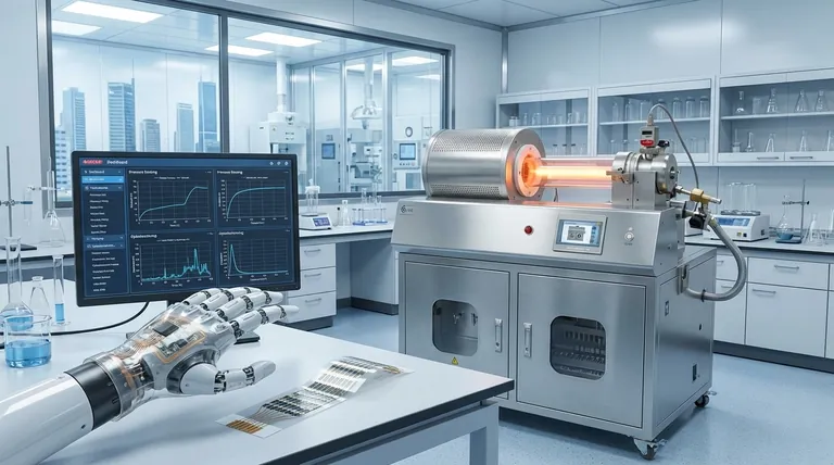
Prototypical devices with commercial potential have already been demonstrated, including touch modules on robot hands for braille recognition and smart gloves that can record and translate sign language.
Optoelectronics and Photodetection
The performance of photodetectors and other optical electronics is highly dependent on the quality of the material interfaces.
PECVD's transfer-free process provides pristine, clean interfaces between the 2D material and the device substrate, enabling the fabrication of high-performance photodetectors.
Biochemical and Molecular Sensing
The high surface-area-to-volume ratio of 2D materials makes them excellent candidates for sensing applications.
PECVD allows for the direct synthesis of these materials on sensor chips, creating a foundation for highly sensitive biochemical sensors and platforms for Surface-Enhanced Raman Spectroscopy (SERS).
Understanding the Trade-offs and Challenges
While highly promising, PECVD is not without its own set of technical considerations. Acknowledging these challenges is key to its successful implementation.
The Challenge of Scalability
While PECVD is considered industrially compatible, scaling a process from a laboratory setup to high-volume manufacturing with perfect uniformity and repeatability remains a significant engineering hurdle.
Optimizing Material Quality
Achieving the perfect, defect-free crystalline quality of the best high-temperature CVD methods can be challenging with PECVD. The process requires careful optimization of plasma conditions, gas chemistry, and power to produce high-quality materials consistently.
Process Complexity
Managing a plasma environment adds a layer of complexity compared to purely thermal processes. Controlling the interactions between precursor gases and the plasma requires a deep understanding of the underlying physics and chemistry to achieve desired results.
Making the Right Choice for Your Goal
Selecting a fabrication method depends entirely on the end goal of your project. PECVD offers a unique combination of benefits that makes it the optimal choice for specific outcomes.
- If your primary focus is device integration and flexibility: PECVD is a superior choice because its low-temperature, transfer-free process allows direct growth on sensitive or flexible substrates.
- If your primary focus is ultimate material purity for fundamental research: Traditional high-temperature CVD may still be preferred for creating the most pristine, large-area single crystals, though it comes with transfer-related challenges.
- If your primary focus is cost-effective, scalable production: PECVD presents a clear path to industrial-scale manufacturing due to its compatibility with existing semiconductor fabrication processes.
Ultimately, PECVD is the key technology that bridges the gap between the extraordinary properties of 2D materials and their practical, real-world implementation.
Summary Table:
| Application Area | Key Advantages | Example Devices |
|---|---|---|
| Advanced Sensors | Direct growth on flexible substrates, high sensitivity | Distributed pressure sensor arrays, electronic skins, smart gloves |
| Optoelectronics | Pristine interfaces, enhanced performance | High-performance photodetectors |
| Biochemical Sensing | Large surface area, direct synthesis on chips | Biochemical sensors, SERS platforms |
Ready to integrate PECVD-prepared 2D materials into your advanced devices? Contact KINTEK today to leverage our exceptional R&D and in-house manufacturing for high-temperature furnace solutions like CVD/PECVD Systems. We offer deep customization to precisely meet your unique experimental needs—get in touch now and transform your lab's capabilities!
Visual Guide

Related Products
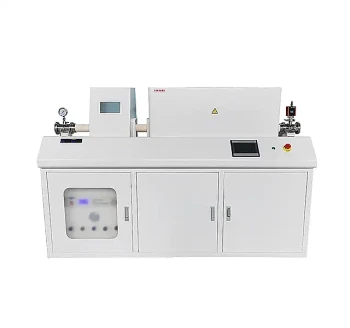
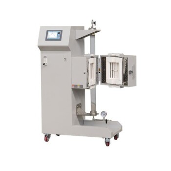
- Inclined Rotary Plasma Enhanced Chemical Deposition PECVD Tube Furnace Machine
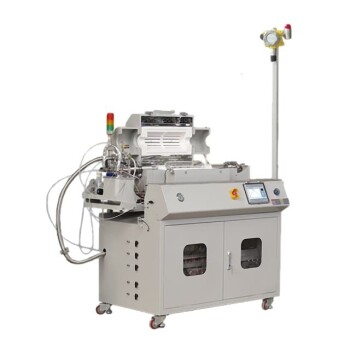
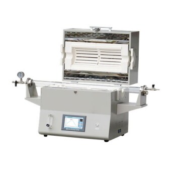
- Slide PECVD Tube Furnace with Liquid Gasifier PECVD Machine
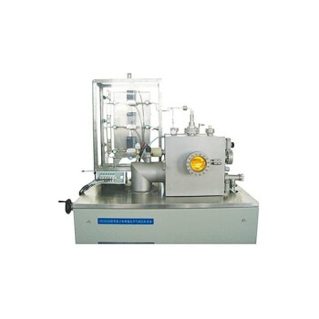
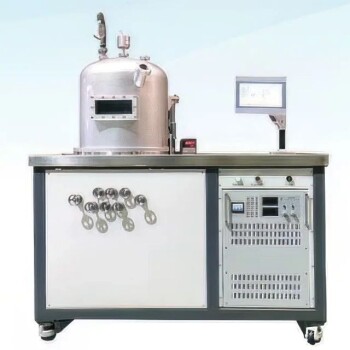
- RF PECVD System Radio Frequency Plasma Enhanced Chemical Vapor Deposition
- Inclined Rotary Plasma Enhanced Chemical Deposition PECVD Tube Furnace Machine
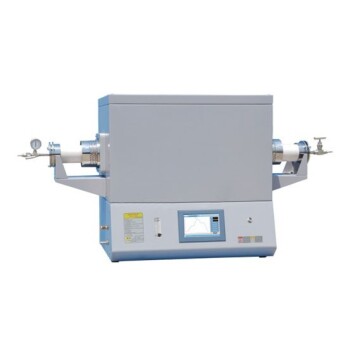
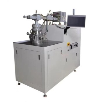
- Custom Made Versatile CVD Tube Furnace Chemical Vapor Deposition CVD Equipment Machine
People Also Ask
- What is the technical objective of using a ceramic rotary rocking device during the glass melting process? Achieve Uniformity
- What is the difference between PVD and PECVD? Choose the Right Thin-Film Coating Technology
- What advantages does the Laser Chemical Vapor Deposition (LCVD) process offer? High Purity & Precision SiC Fibers
- How does chemical vapour deposition (CVD) differ from PVD? Key Differences in Thin-Film Coating Methods
- What is resistance heating and how is it classified? Discover the Best Method for Your Thermal Needs

