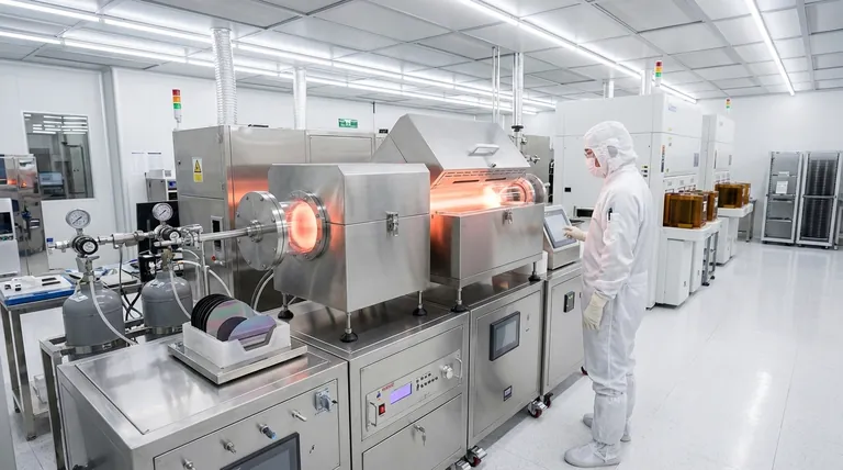
In semiconductor manufacturing, PECVD is the workhorse technology for depositing the essential insulating films that make modern microchips possible. Its primary applications are creating high-quality layers of silicon dioxide (SiO₂) and silicon nitride (Si₃N₄), which serve to isolate conductive pathways, build capacitors, and protect the finished device from the environment. The key advantage of Plasma-Enhanced Chemical Vapor Deposition (PECVD) is its ability to perform this deposition at low temperatures, preserving the delicate, multi-layered circuitry already built on the silicon wafer.
Modern chip fabrication is like building a skyscraper with billions of tiny, fragile electrical components on every floor. PECVD is the critical technique that allows manufacturers to add new insulating layers (the floors and walls) without the intense heat that would melt and destroy the intricate wiring already installed below.
The Fundamental Problem PECVD Solves
The core challenge in building integrated circuits is stacking dozens of functional layers on top of one another. Each new layer must be added without damaging the billions of transistors and wires already fabricated.
The Need for Low-Temperature Deposition
As a chip is built, it accumulates temperature-sensitive components. Traditional Chemical Vapor Deposition (CVD) requires very high temperatures (600-800°C or more) to provide the energy needed to break down precursor gases and form a film.
This level of heat would destroy or alter the properties of previously fabricated structures, such as aluminum interconnects or precisely doped silicon regions. PECVD solves this by operating at much lower temperatures, typically in the 200-400°C range.
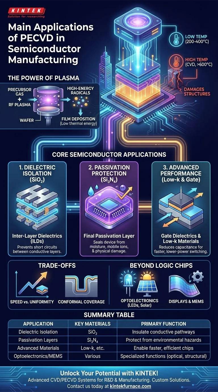
The Role of Plasma
PECVD replaces extreme heat with energy from a plasma. By applying an electromagnetic field (usually radio frequency), precursor gases are ionized into a reactive plasma.
This plasma contains high-energy electrons that collide with gas molecules, breaking them down into reactive radicals. These radicals are highly energetic and readily react on the wafer surface to form a high-quality film, all without needing high thermal energy.
Core Applications in Device Fabrication
PECVD is not used for just one task; it is a versatile tool applied at multiple critical stages of chip manufacturing. Its main function is always the deposition of dielectric (insulating) films.
Dielectric Layers for Isolation
The most common application is depositing silicon dioxide (SiO₂). Think of this as the insulation around the microscopic copper or aluminum "wires" (interconnects) that run throughout the chip.
These Inter-Layer Dielectrics (ILDs) prevent electrical signals from short-circuiting between adjacent or vertically stacked conductive layers, ensuring signals go where they are intended.
Passivation Layers for Protection
Silicon nitride (Si₃N₄) is another key film deposited by PECVD. It is incredibly dense and robust, making it an ideal final passivation layer.
This layer acts as a hard, protective shell over the completed integrated circuit. It seals the device from moisture, mobile ions (like sodium), and physical damage during packaging and use, which is critical for long-term reliability.
Gate Dielectrics and Low-k Materials
In some applications, PECVD is used to deposit the gate dielectric, the ultra-thin insulating layer that controls the flow of current in a transistor.
For advanced chips, PECVD is also used to deposit low-k dielectrics. These are specialized materials with a lower dielectric constant than traditional SiO₂, which reduces parasitic capacitance between wires, allowing for faster switching speeds and lower power consumption.
Understanding the Trade-offs
While indispensable, PECVD is not a perfect solution for every scenario. Understanding its limitations is key to appreciating its role.
Speed vs. Uniformity
PECVD offers very fast deposition rates, which is a major advantage for high-volume manufacturing throughput.
However, achieving the highest speeds can sometimes come at the cost of film uniformity, where the thickness of the deposited layer varies slightly across the wafer. Process engineers must carefully tune parameters to balance this trade-off.
Conformal Coverage
Conformality refers to a film's ability to evenly coat the bottom and sidewalls of complex, three-dimensional trenches and structures.
While PECVD provides good conformal coverage, it is generally less perfect than films deposited by higher-temperature methods like Low-Pressure CVD (LPCVD). For structures requiring near-perfect conformality, other methods may be chosen.
Beyond Mainstream Logic Chips
The versatility of PECVD extends its use to a wide range of other semiconductor devices that are critical to the modern electronics ecosystem.
Optoelectronics: LEDs and Solar Cells
PECVD is essential for manufacturing High-Brightness LEDs and solar cells. It is used to deposit anti-reflective coatings, passivation layers, and transparent conductive oxides that are crucial for managing light and extracting energy efficiently.
Displays and MEMS
The Thin-Film Transistors (TFTs) that control each pixel in modern LCD and OLED displays are often fabricated using PECVD.
It is also a key process in fabricating Micro-Electro-Mechanical Systems (MEMS), such as the tiny accelerometers found in your smartphone, by depositing the structural and sacrificial layers needed to build these microscopic machines.
Making the Right Choice for Your Goal
The specific application of PECVD is always tied to a precise engineering goal.
- If your primary focus is speed and power efficiency in advanced chips: You will use PECVD to deposit low-k dielectric films between dense interconnects to minimize signal delay.
- If your primary focus is device reliability and longevity: You will use PECVD to deposit a final, robust silicon nitride passivation layer to protect the chip from environmental hazards.
- If your primary focus is high-volume, cost-effective manufacturing: PECVD's fast deposition rates make it the go-to process for building the bulk of the insulating layers in a standard chip.
- If your primary focus is specialized optical or mechanical devices: You will leverage PECVD for depositing films with specific optical properties in LEDs or structural layers in MEMS.
Understanding these applications reveals that PECVD is not just a single step, but a foundational pillar enabling the complexity and reliability of nearly all modern semiconductor devices.
Summary Table:
| Application | Key Materials | Primary Function |
|---|---|---|
| Dielectric Layers for Isolation | Silicon Dioxide (SiO₂) | Insulate conductive pathways to prevent short circuits |
| Passivation Layers for Protection | Silicon Nitride (Si₃N₄) | Protect chips from moisture, ions, and physical damage |
| Gate Dielectrics and Low-k Materials | Low-k Dielectrics | Reduce capacitance for faster, lower-power chips |
| Optoelectronics and MEMS | Various (e.g., anti-reflective coatings) | Enable LEDs, solar cells, displays, and sensors |
Unlock the full potential of PECVD for your semiconductor projects with KINTEK! Leveraging exceptional R&D and in-house manufacturing, we provide advanced high-temperature furnace solutions, including CVD/PECVD Systems, tailored to meet the unique needs of semiconductor labs, MEMS developers, and optoelectronics researchers. Our deep customization capabilities ensure precise alignment with your experimental goals, enhancing reliability and efficiency. Contact us today to discuss how our expertise can drive your innovations forward!
Visual Guide
Related Products
- Slide PECVD Tube Furnace with Liquid Gasifier PECVD Machine
- RF PECVD System Radio Frequency Plasma Enhanced Chemical Vapor Deposition
- Inclined Rotary Plasma Enhanced Chemical Deposition PECVD Tube Furnace Machine
- Inclined Rotary Plasma Enhanced Chemical Deposition PECVD Tube Furnace Machine
- Multi Heating Zones CVD Tube Furnace Machine for Chemical Vapor Deposition Equipment
People Also Ask
- In which industries is the tube furnace commonly used? Essential for Materials Science, Energy, and More
- How does a hydrogen reduction environment in an industrial tube furnace facilitate gold-copper alloy microspheres?
- What is plasma in the context of PECVD? Unlock Low-Temperature Thin Film Deposition
- What are the advantages of using a tube furnace CVD system for Cu(111)/graphene? Superior Scalability and Quality
- What plasma source is used in PE-CVD tube furnaces? Unlock Low-Temperature, High-Quality Deposition


