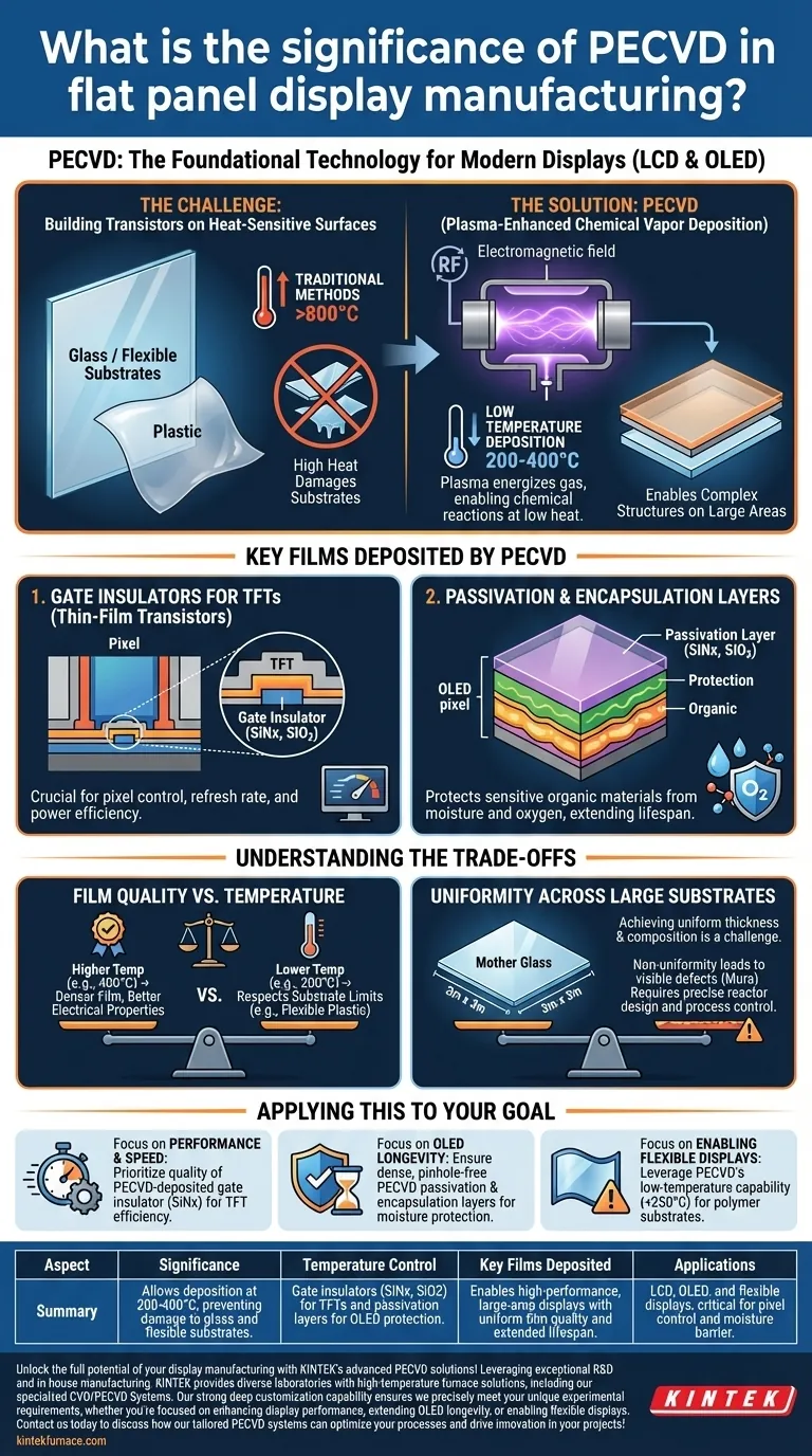
In modern display manufacturing, Plasma-Enhanced Chemical Vapor Deposition (PECVD) is not just an ancillary process; it is a foundational technology. It enables the creation of the microscopic electronic structures, specifically thin-film transistors (TFTs), that control every single pixel on LCD and OLED screens. Without PECVD, the high-performance, large-area displays we use daily would be commercially unviable.
The core significance of PECVD is its ability to deposit high-quality, electronically-critical thin films at low temperatures. This low-temperature capability is what allows complex semiconductor structures to be built on large, heat-sensitive substrates like glass or flexible plastic, which would be damaged or warped by traditional high-temperature methods.
The Core Challenge: Building Transistors on Glass
To understand PECVD's role, you must first understand the fundamental problem of display manufacturing: it involves semiconductor fabrication on a massive, non-traditional surface.
Why Temperature is the Limiting Factor
Unlike semiconductor chips built on small, robust silicon wafers, flat panel displays are manufactured on enormous sheets of glass or flexible polymers.
These substrates have a low thermal budget. Glass can warp, and plastic will melt if subjected to the high temperatures (often >800°C) used in traditional semiconductor deposition processes.
How PECVD Solves the Temperature Problem
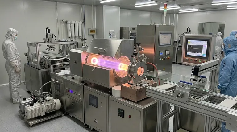
PECVD circumvents the need for high thermal energy by using plasma. An electromagnetic field (typically radio frequency) energizes a gas mixture, creating a plasma.
This plasma contains highly reactive ions and radicals that can deposit as a thin film on the substrate's surface. The plasma, not extreme heat, provides the energy required for the chemical reactions, allowing deposition to occur at much lower temperatures (typically 200-400°C).
Key Films Deposited by PECVD in Displays
PECVD is used to create several distinct layers, each with a critical function in the display's pixel architecture.
Gate Insulators for Thin-Film Transistors (TFTs)
Every pixel in an active-matrix display is controlled by at least one TFT, which acts as a tiny switch. A critical component of this switch is the gate insulator.
PECVD is used to deposit dielectric materials like silicon nitride (SiNx) and silicon dioxide (SiO2) to form this insulating layer. The quality of this film directly impacts the transistor's performance, influencing factors like screen refresh rate and power consumption.
Passivation and Encapsulation Layers
Displays contain sensitive materials that degrade rapidly when exposed to oxygen and moisture. This is especially true for the organic materials in an OLED display.
PECVD deposits dense, pinhole-free layers of silicon nitride or silicon dioxide over the active electronics. This passivation layer acts as a robust barrier, protecting the delicate components and dramatically increasing the operational lifetime of the display.
Understanding the Trade-offs
While indispensable, PECVD is a process governed by engineering compromises that affect cost, speed, and final quality.
Film Quality vs. Deposition Temperature
There is a direct relationship between the deposition temperature and the quality of the resulting film. While PECVD is a "low-temperature" process, films deposited at the higher end of its range (e.g., 400°C) are generally denser and have better electrical properties than those deposited at lower temperatures (e.g., 200°C).
Choosing the right temperature is a balancing act between achieving the required film quality and respecting the thermal limits of the substrate, especially for flexible plastic displays.
Uniformity Across Large Substrates
Modern display fabrication plants use "mother glass" substrates that can be over 3 meters by 3 meters. Achieving a perfectly uniform film thickness and composition across such a vast area is a significant engineering challenge.
Non-uniformity can lead to variations in transistor performance across the display, resulting in visible defects like uneven brightness (mura). Reactor design and process control are critical to maintaining this uniformity.
Applying This to Your Goal
Your focus determines which aspect of the PECVD process is most critical.
- If your primary focus is display performance and speed: The quality of the PECVD-deposited gate insulator (SiNx) is paramount, as it dictates the electrical efficiency of the pixel's TFT.
- If your primary focus is OLED display longevity: The density and integrity of the PECVD passivation and encapsulation layers are the most important factors for preventing moisture-induced degradation.
- If your primary focus is enabling flexible displays: The ability of PECVD to deposit functional electronic layers at very low temperatures (<250°C) is the key enabler, allowing for the use of polymer substrates.
Ultimately, PECVD is the crucial technology that translates the principles of microelectronics to the macro scale of flat panel displays.
Summary Table:
| Aspect | Significance |
|---|---|
| Temperature Control | Allows deposition at 200-400°C, preventing damage to glass and flexible substrates. |
| Key Films Deposited | Gate insulators (SiNx, SiO2) for TFTs and passivation layers for OLED protection. |
| Benefits | Enables high-performance, large-area displays with uniform film quality and extended lifespan. |
| Applications | LCD, OLED, and flexible displays, critical for pixel control and moisture barrier. |
Unlock the full potential of your display manufacturing with KINTEK's advanced PECVD solutions!
Leveraging exceptional R&D and in-house manufacturing, KINTEK provides diverse laboratories with high-temperature furnace solutions, including our specialized CVD/PECVD Systems. Our strong deep customization capability ensures we precisely meet your unique experimental requirements, whether you're focused on enhancing display performance, extending OLED longevity, or enabling flexible displays.
Contact us today to discuss how our tailored PECVD systems can optimize your processes and drive innovation in your projects!
Visual Guide
Related Products
- RF PECVD System Radio Frequency Plasma Enhanced Chemical Vapor Deposition
- Slide PECVD Tube Furnace with Liquid Gasifier PECVD Machine
- Inclined Rotary Plasma Enhanced Chemical Deposition PECVD Tube Furnace Machine
- Inclined Rotary Plasma Enhanced Chemical Deposition PECVD Tube Furnace Machine
- Cylindrical Resonator MPCVD Machine System for Lab Diamond Growth
People Also Ask
- What is RF in PECVD? A Critical Control for Plasma Deposition
- What are the advantages of PECVD in film deposition? Achieve Low-Temp, High-Quality Coatings
- What are some promising applications of PECVD-prepared 2D materials? Unlock Advanced Sensing and Optoelectronics
- What is the role of RF power in PECVD and how does the RF-PECVD process work? Master Thin Film Deposition Control
- What are the key advantages of PECVD technology? Achieve Low-Temperature, High-Quality Thin Film Deposition


