In semiconductor fabrication, the primary difference between Plasma-Enhanced Chemical Vapor Deposition (PECVD) and traditional Chemical Vapor Deposition (CVD) is the energy source used to drive the reaction. While traditional CVD relies exclusively on high thermal energy (heat) to break down precursor gases, PECVD uses an energized plasma to achieve the same result at significantly lower temperatures. This distinction is not merely academic; it fundamentally changes what materials can be processed and the quality of the resulting films.
The core choice between PECVD and traditional CVD hinges on your process's thermal budget. PECVD's use of plasma decouples the chemical reaction from high heat, enabling the deposition of high-quality thin films on temperature-sensitive substrates that would be destroyed by traditional CVD methods.

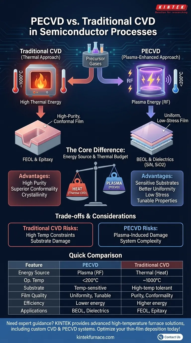
The Fundamental Difference: Energy Source
The method used to supply energy to the precursor gases dictates the operating conditions and capabilities of the deposition process.
Traditional CVD: The Thermal Approach
Traditional CVD is conceptually straightforward. Precursor gases are introduced into a high-temperature furnace, typically operating around 1,000°C. This intense heat provides the necessary activation energy to break the chemical bonds in the gases, allowing them to react and deposit as a solid thin film on the substrate.
PECVD: The Plasma-Enhanced Approach
PECVD introduces a third component: plasma. Plasma is an ionized gas, a high-energy state of matter created by applying a strong electromagnetic field (typically radio frequency) to the precursor gases.
This plasma, not intense heat, provides the energy to break down the gas molecules into reactive radicals. Because the energy comes from the plasma, the substrate itself can remain at a much lower temperature, often below 200°C.
Key Advantages of the PECVD Process
The ability to operate at low temperatures gives PECVD several critical advantages in modern semiconductor manufacturing.
Enabling Deposition on Sensitive Substrates
This is the most significant benefit of PECVD. Many advanced devices are built with materials—like certain metals, polymers, or low-k dielectrics—that cannot withstand the high temperatures of traditional CVD.
PECVD allows for the deposition of essential insulating or passivation layers on top of these completed structures without causing damage, degradation, or thermal stress that could lead to wafer warpage.
Superior Film Quality and Control
Because the deposition is not driven by brute-force heat, PECVD offers finer control over the reaction. This results in films with better uniformity, lower stress, and a reduced likelihood of cracking. The energy from the plasma can be tuned to optimize film properties like density and chemical composition (stoichiometry).
Improved Process Efficiency
The lower operating temperatures directly translate to lower energy consumption, making the process more cost-effective. Additionally, some PECVD processes can result in less unwanted deposition on chamber walls, simplifying maintenance and cleaning cycles.
Understanding the Trade-offs
While PECVD is dominant in many applications, it is not a universal replacement for traditional CVD. An expert must understand the potential downsides.
When Thermal CVD Excels: Purity and Con-formality
For certain applications, particularly in the front-end-of-line (FEOL), traditional high-temperature CVD can produce films of exceptional purity and crystallinity. Processes like epitaxial silicon growth require the highly ordered structure that a thermal process enables.
Furthermore, thermal CVD often provides superior con-formality, meaning the film coats complex, high-aspect-ratio trenches and structures more uniformly than some PECVD processes.
The Risk of Plasma-Induced Damage
The high-energy ions within the plasma that enable the low-temperature reaction can also be a source of damage. This ion bombardment can introduce defects into the substrate surface or the growing film, which can be detrimental to the performance of sensitive electronic devices.
System Complexity and Cost
PECVD reactors are inherently more complex than their traditional thermal counterparts. They require sophisticated RF power generators, impedance matching networks, and advanced gas distribution systems (showerheads) to create and sustain a stable, uniform plasma. This increases both the initial capital cost and the ongoing maintenance complexity.
Making the Right Choice for Your Process
Selecting the correct deposition method requires a clear understanding of your specific film requirements and substrate limitations.
- If your primary focus is depositing on temperature-sensitive materials: PECVD is the definitive and often only choice, especially for back-end-of-line (BEOL) processes involving metal interconnects.
- If your primary focus is the highest possible film purity and crystallinity for foundational layers: Traditional high-temperature CVD is often the superior method for tasks like epitaxy.
- If your primary focus is depositing standard dielectric films (SiN, SiO2) with good quality and high throughput: PECVD is the industry standard due to its balance of quality, speed, and low thermal budget.
Understanding the fundamental trade-off between thermal energy and plasma energy is the key to mastering modern thin-film deposition.
Summary Table:
| Feature | PECVD | Traditional CVD |
|---|---|---|
| Energy Source | Plasma (RF) | Thermal (Heat) |
| Operating Temperature | Low (e.g., <200°C) | High (e.g., ~1000°C) |
| Substrate Compatibility | Temperature-sensitive materials (e.g., metals, polymers) | High-temperature tolerant materials |
| Film Quality | Better uniformity, lower stress, tunable properties | Higher purity, superior con-formality, crystallinity |
| Process Efficiency | Lower energy use, reduced chamber deposition | Higher energy consumption, simpler system |
| Applications | BEOL processes, dielectric films (SiN, SiO2) | FEOL processes, epitaxial growth |
Need expert guidance on selecting the right CVD system for your semiconductor processes? At KINTEK, we leverage exceptional R&D and in-house manufacturing to provide advanced high-temperature furnace solutions, including PECVD and traditional CVD systems. Our product line—featuring Muffle, Tube, Rotary Furnaces, Vacuum & Atmosphere Furnaces, and CVD/PECVD Systems—is complemented by strong deep customization capabilities to precisely meet your unique experimental requirements. Contact us today to optimize your thin-film deposition and enhance your lab's efficiency!
Visual Guide
Related Products
- RF PECVD System Radio Frequency Plasma Enhanced Chemical Vapor Deposition
- Inclined Rotary Plasma Enhanced Chemical Deposition PECVD Tube Furnace Machine
- Inclined Rotary Plasma Enhanced Chemical Deposition PECVD Tube Furnace Machine
- Slide PECVD Tube Furnace with Liquid Gasifier PECVD Machine
- Custom Made Versatile CVD Tube Furnace Chemical Vapor Deposition CVD Equipment Machine
People Also Ask
- How is silicon dioxide deposited from tetraethylorthosilicate (TEOS) in PECVD? Achieve Low-Temperature, High-Quality SiO2 Films
- What are the key advantages of PECVD technology? Achieve Low-Temperature, High-Quality Thin Film Deposition
- What are the applications of plasma enhanced chemical vapor deposition? Key Uses in Electronics, Optics & Materials
- What is PECVD specification? A Guide to Choosing the Right System for Your Lab
- What is RF in PECVD? A Critical Control for Plasma Deposition


