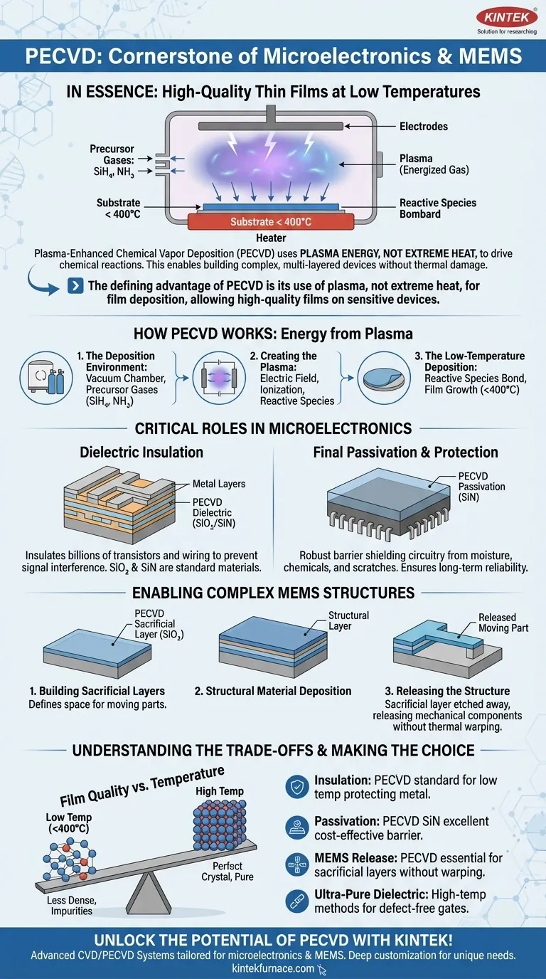
In essence, Plasma-Enhanced Chemical Vapor Deposition (PECVD) is a cornerstone of microfabrication because it enables the deposition of high-quality thin films at low temperatures. These films are used to create critical insulation, protective passivation layers, and temporary structural molds in both microelectronic circuits and Micro-Electro-Mechanical Systems (MEMS). This low-temperature capability is the key to building complex, multi-layered devices without damaging previously fabricated components.
The defining advantage of PECVD is its use of plasma, not extreme heat, to drive the chemical reactions needed for film deposition. This allows for the growth of high-quality insulating and protective films on sensitive devices without causing the thermal damage that would occur with higher-temperature methods.
How PECVD Works: Energy from Plasma, Not Heat
To understand PECVD's role, you must first understand its fundamental mechanism. Unlike traditional Chemical Vapor Deposition (CVD) which relies on high temperatures to break down gases, PECVD uses an energized gas called a plasma.
The Deposition Environment
The process takes place inside a vacuum chamber. Precursor gases, such as silane (SiH₄) for silicon films or ammonia (NH₃) for nitride films, are introduced into this low-pressure environment.
Creating the Plasma
An electric field is applied between two electrodes inside the chamber. This field energizes free electrons, causing them to collide with neutral gas molecules. These collisions transfer energy, stripping electrons from the molecules and creating a mix of ions, electrons, and highly reactive neutral species known as plasma.
The Low-Temperature Deposition
These plasma-generated reactive species are far more chemically active than their original gas molecules. When they come into contact with the surface of the substrate (the silicon wafer), they readily bond and form a solid, uniform thin film. Because the plasma provides the energy for the reaction, the substrate itself can remain at a relatively low temperature, typically below 400°C.
Critical Roles in Microelectronics
In the manufacturing of integrated circuits (chips), PECVD is not just useful; it is essential for creating the device's complex, layered architecture.
Dielectric Insulation
Modern chips contain billions of transistors connected by intricate wiring. To prevent electrical signals from interfering with each other, these components must be separated by insulating materials, or dielectrics. PECVD is the standard method for depositing silicon dioxide (SiO₂) and silicon nitride (SiN) films between metal layers to provide this crucial electrical isolation.
Final Passivation and Protection
The final step in fabricating a chip is to encapsulate it in a protective layer. A film of PECVD silicon nitride serves as a robust barrier, or passivation layer, shielding the delicate circuitry from moisture, chemical contaminants, and minor physical scratches, which ensures the device's long-term reliability.
Enabling Complex MEMS Structures
For MEMS—tiny machines built on a silicon wafer—PECVD's function extends from electrical insulation to mechanical construction.
Building Sacrificial Layers
MEMS often feature moving parts like microscopic cantilevers, gears, or membranes. To create these, a temporary mold is needed. PECVD is used to deposit a sacrificial layer, typically silicon dioxide, which defines the shape of the space underneath the eventual moving part.
Releasing the Mechanical Structure
After the sacrificial layer is in place, the actual structural material of the MEMS device is deposited on top of it. Finally, a specific chemical etchant is used to wash away only the sacrificial layer, leaving the free-standing mechanical component "released" and able to move. The low temperature of PECVD is vital here to prevent warping or stress in these delicate structures.
Understanding the Trade-offs
No process is perfect for every application. Understanding PECVD's limitations is key to using it effectively.
Film Quality vs. Temperature
The primary trade-off is between deposition temperature and film quality. Because PECVD operates at lower temperatures, the deposited atoms have less energy to arrange themselves into a perfect crystal lattice. This means PECVD films are generally less dense and may contain more impurities (like hydrogen) than films grown with high-temperature methods.
When "Good Enough" is Best
For many applications, this slightly lower film quality is an acceptable and logical trade-off. The benefit of avoiding thermal damage to sensitive underlying layers (like aluminum interconnects, which can be damaged above 450°C) far outweighs the need for a perfectly dense film. For roles like inter-metal insulation or final passivation, PECVD's quality is more than sufficient.
Making the Right Choice for Your Goal
Selecting the right deposition technique depends entirely on the specific layer's function within the device.
- If your primary focus is insulating between metal layers in a circuit: PECVD is the industry standard because its low temperature protects the underlying metal wiring from damage.
- If your primary focus is creating a final, robust protective layer for a device: PECVD silicon nitride provides an excellent and cost-effective passivation barrier against environmental hazards.
- If your primary focus is fabricating releasable MEMS components: PECVD is essential for depositing sacrificial layers without inducing thermal stress that could warp the final mechanical structures.
- If your primary focus is creating an ultra-pure, defect-free gate dielectric for a transistor: You would likely use a high-temperature method like thermal oxidation, where film perfection is the absolute top priority.
Ultimately, PECVD's ability to deposit functional films without the damaging effects of heat is what makes the complexity of modern microelectronic and MEMS devices possible.
Summary Table:
| Application Area | Key PECVD Contributions | Common Materials Deposited |
|---|---|---|
| Microelectronics | Dielectric insulation, passivation layers | Silicon dioxide (SiO₂), silicon nitride (SiN) |
| MEMS Devices | Sacrificial layers for structural release | Silicon dioxide (SiO₂) |
| General Benefits | Low-temperature operation, high-quality thin films | Various insulating and protective films |
Unlock the potential of PECVD for your lab with KINTEK! Leveraging exceptional R&D and in-house manufacturing, we provide advanced high-temperature furnace solutions, including CVD/PECVD Systems, tailored for diverse laboratories. Our strong deep customization capability ensures we precisely meet your unique experimental needs for microelectronics and MEMS applications. Contact us today to enhance your fabrication processes and achieve superior results!
Visual Guide
Related Products
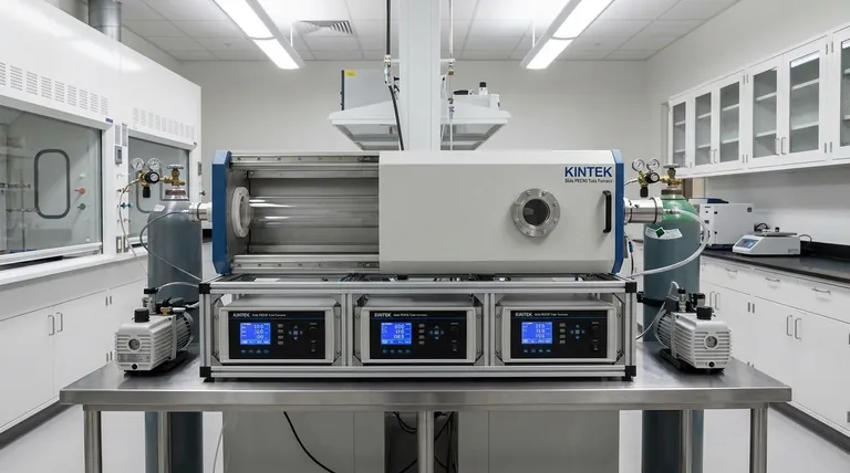
- Slide PECVD Tube Furnace with Liquid Gasifier PECVD Machine
- RF PECVD System Radio Frequency Plasma Enhanced Chemical Vapor Deposition
- Inclined Rotary Plasma Enhanced Chemical Deposition PECVD Tube Furnace Machine
- Inclined Rotary Plasma Enhanced Chemical Deposition PECVD Tube Furnace Machine
- Multi Heating Zones CVD Tube Furnace Machine for Chemical Vapor Deposition Equipment
People Also Ask
- How does a hydrogen reduction environment in an industrial tube furnace facilitate gold-copper alloy microspheres?
- What are the disadvantages of tube furnace cracking when processing heavy raw materials? Avoid Costly Downtime and Inefficiency
- What are the typical conditions for plasma-enhanced CVD processes? Achieve Low-Temperature Thin Film Deposition
- What plasma source is used in PE-CVD tube furnaces? Unlock Low-Temperature, High-Quality Deposition
- How does PECVD equipment contribute to TOPCon bottom cells? Mastering Hydrogenation for Maximum Solar Efficiency


