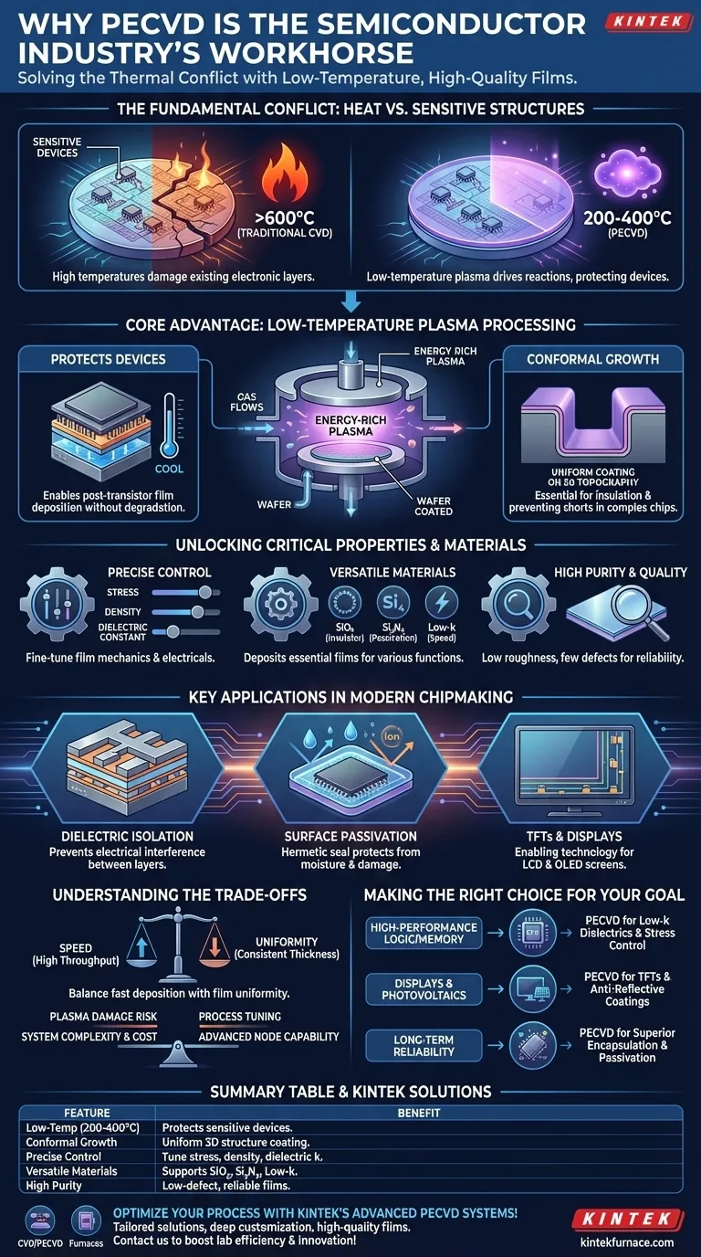
At its core, Plasma-Enhanced Chemical Vapor Deposition (PECVD) is highly regarded in the semiconductor industry because it solves a fundamental conflict: the need to deposit high-quality, functional thin films without using the high temperatures that would damage the intricate, sensitive electronic structures already built on a silicon wafer. This low-temperature capability, combined with precise control over film properties, makes it an indispensable tool for fabricating modern microelectronic devices.
PECVD's primary value lies in its ability to enable the creation of essential insulating and protective layers on a semiconductor chip after temperature-sensitive transistors have been formed, a task that is impossible with high-heat alternatives.
The Core Advantage: Low-Temperature Processing
The defining feature of PECVD is its use of an energy-rich plasma to drive chemical reactions instead of relying solely on thermal energy. This shift has profound implications for semiconductor manufacturing.
Protecting Temperature-Sensitive Devices
As integrated circuits (ICs) become more complex, they are built up in dozens of layers. Early layers often contain delicate transistors that cannot withstand the high temperatures (often >600°C) required by traditional Chemical Vapor Deposition (CVD).
PECVD operates at much lower temperatures (typically 200-400°C), allowing for the deposition of critical films later in the manufacturing flow without degrading or altering the performance of underlying components.
Enabling Conformal Film Growth
The plasma-driven process allows for conformal deposition, meaning the film can evenly coat the complex, three-dimensional topography of a modern chip, including the vertical sidewalls of trenches. This is essential for ensuring complete insulation and preventing electrical shorts between conductive layers.
Unlocking Critical Film Properties and Materials
Beyond its low-temperature advantage, PECVD provides engineers with a high degree of control over the final product, which is vital for performance and reliability.
Precise Control Over Film Characteristics
Engineers can finely tune process parameters like gas flow, pressure, and plasma power. This allows for precise control over key mechanical and electrical properties of the deposited film, such as its stress, density, and dielectric constant. Managing film stress is particularly critical to prevent wafer bowing or film cracking.
A Versatile Material Deposition Tool
PECVD is not limited to one type of material. It is widely used to deposit some of the most important films in semiconductor fabrication:
- Silicon Dioxide (SiO₂): A fundamental insulator used to isolate conductive layers.
- Silicon Nitride (Si₃N₄): A robust insulator and barrier layer used for passivation and encapsulation.
- Low-k Dielectrics: Advanced materials with a lower dielectric constant than SiO₂, used to reduce parasitic capacitance between wires, enabling faster and more power-efficient chips.
Ensuring High Purity and Quality
The controlled environment of a PECVD chamber ensures that the deposited films have minimal impurity levels. The process delivers high-quality films with low roughness and few defects or voids, which are essential for the reliability and yield of multi-billion transistor chips.
Key Applications in Modern Chipmaking
PECVD is not a niche process; it is a workhorse used for several mission-critical steps in producing semiconductors, displays, and optical devices.
Dielectric Isolation
The primary application of PECVD is depositing insulating (dielectric) films. These layers separate the vast, dense network of metal interconnects and capacitors within an IC, preventing electrical interference and short circuits.
Surface Passivation and Encapsulation
After the active circuitry is built, a final layer of silicon nitride is often deposited using PECVD. This layer acts as a durable, hermetic seal that passivates the surface, protecting the sensitive chip from moisture, mobile ions, and physical damage during packaging and operation.
Building Advanced Components
PECVD's utility extends beyond basic insulation. It is a key enabling technology for producing thin-film transistors (TFTs), which are the building blocks of modern flat-panel displays (LCD and OLED). It is also used to create anti-reflective layers for optical components and solar cells.
Understanding the Trade-offs
While powerful, PECVD is not without its considerations. A true technical understanding requires acknowledging its limitations.
Speed vs. Uniformity
PECVD systems are capable of very fast deposition rates, which is excellent for manufacturing throughput. However, pushing for maximum speed can sometimes compromise the uniformity of the film's thickness across the entire diameter of the wafer. Engineers must carefully balance this trade-off.
Potential for Plasma-Induced Damage
While the low temperature protects devices from thermal damage, the high-energy plasma itself can sometimes cause subtle damage to the wafer's surface if not meticulously controlled. This requires sophisticated process tuning to mitigate.
System Complexity and Cost
PECVD systems are complex, high-vacuum machines that represent a significant capital investment. Their operational costs are also higher than some simpler deposition methods, a cost justified by the unique capabilities they provide for advanced node manufacturing.
Making the Right Choice for Your Goal
The decision to use PECVD is driven by the specific requirements of the device being fabricated.
- If your primary focus is high-performance logic and memory: PECVD is non-negotiable for depositing the low-k dielectric insulators and stress-controlled liners required for speed and miniaturization.
- If your primary focus is displays or photovoltaics: PECVD is the go-to method for creating the essential TFT backplanes and anti-reflective coatings on temperature-sensitive glass or flexible substrates.
- If your primary focus is long-term device reliability: PECVD provides the superior encapsulation and passivation films needed to protect the final product from environmental and mechanical failure.
Ultimately, PECVD's strategic balance of low-temperature processing, material versatility, and high-quality results makes it an irreplaceable pillar of modern semiconductor manufacturing.
Summary Table:
| Feature | Benefit |
|---|---|
| Low-Temperature Processing (200-400°C) | Protects sensitive devices, enables post-transistor film deposition |
| Conformal Film Growth | Ensures uniform coating on 3D structures, preventing electrical shorts |
| Precise Control of Film Properties | Allows tuning of stress, density, and dielectric constant for optimal performance |
| Versatile Material Deposition | Supports SiO₂, Si₃N₄, low-k dielectrics for various applications |
| High Purity and Quality | Delivers low-defect films essential for chip reliability and yield |
Optimize your semiconductor processes with KINTEK's advanced PECVD systems! Leveraging exceptional R&D and in-house manufacturing, we provide tailored solutions for diverse laboratories. Our product line, including CVD/PECVD Systems, Muffle, Tube, Rotary Furnaces, and Vacuum & Atmosphere Furnaces, is complemented by strong deep customization capabilities to precisely meet your unique experimental needs. Contact us today to enhance your device fabrication with high-quality, low-temperature thin films and boost your lab's efficiency and innovation!
Visual Guide
Related Products
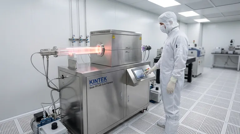
- RF PECVD System Radio Frequency Plasma Enhanced Chemical Vapor Deposition
- Slide PECVD Tube Furnace with Liquid Gasifier PECVD Machine
- Inclined Rotary Plasma Enhanced Chemical Deposition PECVD Tube Furnace Machine
- Inclined Rotary Plasma Enhanced Chemical Deposition PECVD Tube Furnace Machine
- Cylindrical Resonator MPCVD Machine System for Lab Diamond Growth
People Also Ask
- What are the advantages of PECVD in film deposition? Achieve Low-Temp, High-Quality Coatings
- What are the applications of plasma enhanced chemical vapor deposition? Key Uses in Electronics, Optics & Materials
- What are some promising applications of PECVD-prepared 2D materials? Unlock Advanced Sensing and Optoelectronics
- What is PECVD specification? A Guide to Choosing the Right System for Your Lab
- How does film quality compare between PECVD and CVD? Choose the Best Method for Your Substrate


