At its core, the primary advantage of in-situ plasma cleaning in a Plasma-Enhanced Chemical Vapor Deposition (PECVD) system is its ability to restore the chamber to a consistent, pristine state without manual intervention. This automated process significantly increases equipment uptime, improves process repeatability, and prevents defects caused by film accumulation, directly translating to higher yield and more reliable device performance.
Plasma cleaning is not merely a maintenance task; it is a critical process control strategy. It transforms the variable and time-consuming act of manual cleaning into a fast, repeatable, and automated step that is fundamental to achieving stable, high-volume manufacturing.
Why Chamber Cleaning is Non-Negotiable in PECVD
To understand the value of plasma cleaning, you must first understand the problem it solves. The PECVD process is designed to build thin films on a substrate, but it inevitably deposits that same material on all internal chamber surfaces, including the walls, showerhead, and substrate holder.
The Problem of Film Accumulation
With each deposition run, layers of material build up on the chamber hardware. This accumulated film develops internal stress. Eventually, this stress becomes too great, and the material cracks and flakes off into the chamber environment.
The Impact on Process Stability and Yield
These free-floating particles are a primary source of defects. If they land on a wafer during deposition, they can ruin the device being fabricated.
Furthermore, the buildup changes the thermal and electrical properties of the chamber itself. This "process drift" alters the plasma conditions from one run to the next, making consistent film deposition impossible and leading to unpredictable results and lower yields.
How Plasma Cleaning Works: An In-Situ Solution
Plasma cleaning addresses this challenge by using the system's own plasma-generating capability to remove the unwanted film deposits from the chamber walls. It is an in-situ process, meaning it occurs inside the sealed vacuum chamber between deposition runs.
Turning Deposition on Its Head
Think of plasma cleaning as the reverse of deposition. Instead of precursor gases that build a solid film, a cleaning gas (such as a fluorine-based compound) is introduced into the chamber.
The system's RF power energizes this gas, creating a plasma filled with highly reactive species (ions and radicals). These species react with the solid film deposited on the chamber walls, converting it into a volatile gaseous byproduct that is safely removed by the vacuum pump.
The Critical Role of End-Point Detection
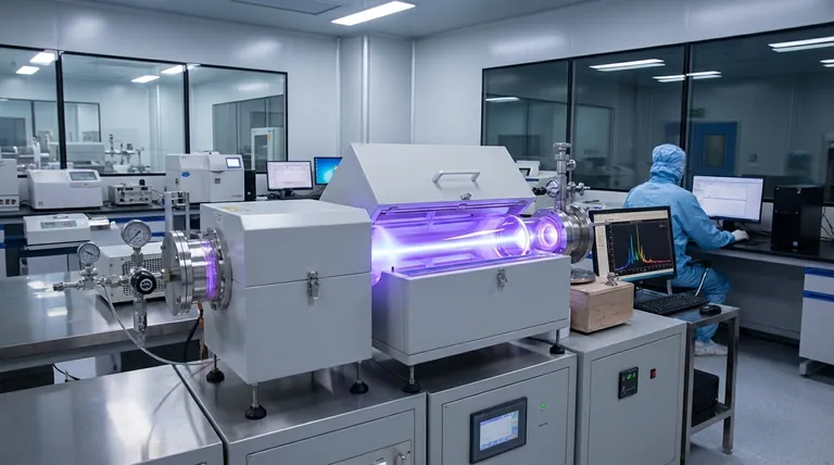
Modern systems use end-point control to optimize this process. An optical emission spectrometer (OES) monitors the light, or "glow," emitted by the plasma.
The chemical byproducts of the cleaning reaction have a unique spectral signature. When the unwanted film has been fully removed, these byproducts disappear, and the plasma's light signature changes. The OES detects this change and automatically stops the cleaning process, ensuring a perfectly clean chamber without wasting time or gas and preventing damage to chamber components from over-exposure to the plasma.
Understanding the Trade-offs: Plasma vs. Manual Cleaning
While highly effective, it is important to view plasma cleaning in the context of its alternative: a manual "wet" clean.
Advantage: Uptime and Throughput
A manual clean is a significant downtime event. The chamber must be cooled, vented to atmosphere, physically opened, scrubbed by a technician, and then pumped back down to vacuum. This can take hours.
In contrast, an automated plasma clean typically takes only minutes and occurs between wafer runs without ever breaking vacuum. This maximizes equipment uptime and wafer throughput.
Advantage: Consistency and Repeatability
Manual cleaning is inherently variable, depending on the diligence of the technician. Plasma cleaning is a pre-programmed recipe executed precisely by the machine every time, eliminating human error and ensuring the chamber starts in an identical state before every deposition. This repeatability is essential for process control.
Limitation: Process Development
Developing a robust plasma clean recipe requires expertise. The choice of cleaning gas, power levels, and pressure must be carefully engineered to remove the target film efficiently without damaging the chamber's internal components. An improperly designed recipe can be ineffective or destructive.
Pitfall: Material Selectivity
A plasma clean recipe is highly selective for a specific material. A recipe designed to remove silicon nitride, for example, may be ineffective against silicon dioxide or other films. Running multiple processes in the same chamber may require developing and validating multiple cleaning recipes to manage residue.
Making the Right Choice for Your Goal
Integrating a plasma clean process requires treating it with the same seriousness as the deposition recipe itself.
- If your primary focus is high-volume manufacturing: Automated in-situ plasma cleaning with end-point control is non-negotiable for maximizing uptime, ensuring process stability, and achieving high yields.
- If your primary focus is research and development: While infrequent manual cleans may suffice initially, developing a validated plasma clean recipe is crucial for establishing a repeatable baseline and ensuring your experimental results are consistent.
- If your primary focus is process control: Leveraging end-point detection is the only way to guarantee the chamber is returned to a known, clean state before every run, which is the foundation of a stable process.
Ultimately, viewing the chamber clean not as janitorial work but as the first critical step of your deposition process is the key to mastering PECVD.
Summary Table:
| Aspect | Plasma Cleaning Advantage |
|---|---|
| Uptime | Increases by automating cleaning between runs without breaking vacuum |
| Repeatability | Ensures consistent chamber state, reducing process drift and defects |
| Yield | Improves by preventing particle contamination and process variability |
| Efficiency | Uses end-point detection for precise, fast cleaning cycles |
Elevate your PECVD process with KINTEK's advanced solutions! Leveraging exceptional R&D and in-house manufacturing, we provide diverse laboratories with high-temperature furnace systems, including CVD/PECVD Systems, Muffle, Tube, Rotary, Vacuum & Atmosphere Furnaces. Our strong deep customization capability precisely meets your unique experimental needs, ensuring enhanced uptime, repeatability, and yield. Contact us today to discuss how we can optimize your setup for superior performance and reliability!
Visual Guide

Related Products
- RF PECVD System Radio Frequency Plasma Enhanced Chemical Vapor Deposition
- Slide PECVD Tube Furnace with Liquid Gasifier PECVD Machine
- Inclined Rotary Plasma Enhanced Chemical Deposition PECVD Tube Furnace Machine
- Inclined Rotary Plasma Enhanced Chemical Deposition PECVD Tube Furnace Machine
- MPCVD Machine System Reactor Bell-jar Resonator for Lab and Diamond Growth
People Also Ask
- What are the applications of plasma enhanced chemical vapor deposition? Key Uses in Electronics, Optics & Materials
- What are the advantages of PECVD in film deposition? Achieve Low-Temp, High-Quality Coatings
- How does film quality compare between PECVD and CVD? Choose the Best Method for Your Substrate
- What is the role of RF power in PECVD and how does the RF-PECVD process work? Master Thin Film Deposition Control
- What is PECVD specification? A Guide to Choosing the Right System for Your Lab


