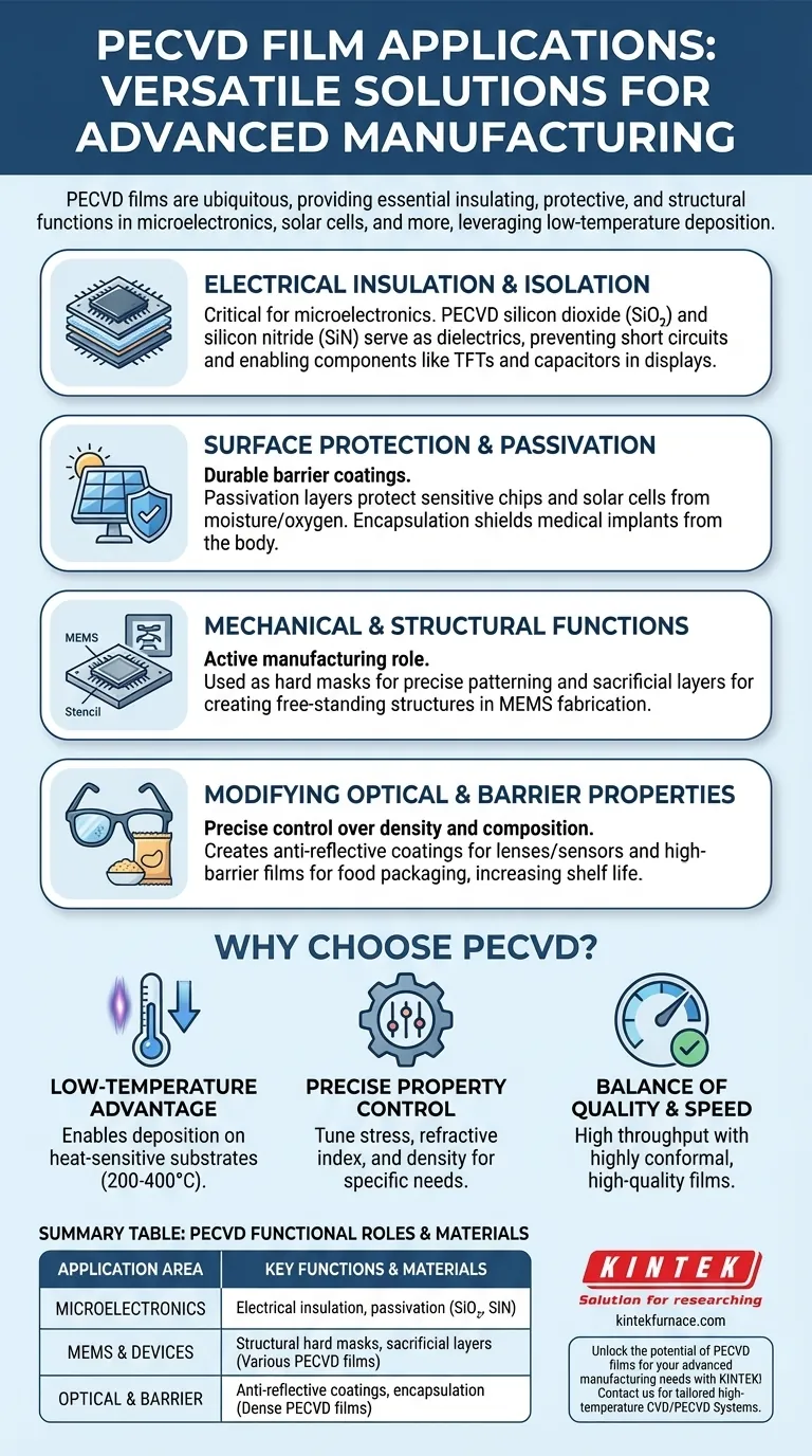
In short, PECVD films are everywhere. They are critical components in semiconductor chips, solar cells, LEDs, and optical devices, where they serve as insulators, protective barriers, and structural elements. Their applications even extend to everyday items like food packaging and medical implants.
The true value of Plasma-Enhanced Chemical Vapor Deposition (PECVD) is not found in a single application, but in its versatility. Its ability to deposit high-quality, functional thin films at low temperatures makes it an indispensable tool across nearly every advanced manufacturing sector.
The Functional Roles of PECVD Films
To understand why PECVD is so widely adopted, it's more useful to think in terms of the function the film provides. Different applications leverage the same core capabilities of PECVD films.
Electrical Insulation and Isolation
The most dominant application of PECVD is in microelectronics, where films are used to control the flow of electricity.
PECVD-deposited silicon dioxide (SiO₂) and silicon nitride (SiN) are excellent electrical insulators, or dielectrics. They are used to isolate conductive layers from each other within an integrated circuit, preventing short circuits.
These films are also fundamental to building components like capacitors and thin-film transistors (TFTs) found in modern displays.
Surface Protection and Passivation
Many devices are highly sensitive to their environment. PECVD films act as a durable shield.
A passivation layer is like a microscopic raincoat for a semiconductor chip or solar cell. It protects the sensitive surface from moisture, oxygen, and other contaminants that could degrade performance and lifespan.
This same principle applies to encapsulation, where PECVD provides a barrier coating for medical implants, protecting them from the body and the body from them.
Mechanical and Structural Functions
PECVD films are not just passive layers; they play an active role in the manufacturing process itself.
In microfabrication, a hard mask is a durable film deposited onto a wafer. This film is patterned and used as a stencil to guide etching, allowing for the creation of precise, microscopic features.
For Micro-Electro-Mechanical Systems (MEMS), PECVD is used to deposit sacrificial layers. These are temporary structural layers that are selectively removed later in the process to create free-standing mechanical parts like cantilevers or membranes.
Modifying Optical and Barrier Properties
PECVD allows for precise control over a film's density and composition, which is ideal for tuning how it interacts with light and other molecules.
Anti-reflective coatings on eyeglass lenses, solar cells, and camera sensors are often deposited using PECVD to maximize light transmission and reduce glare.
In the food packaging industry, a dense PECVD film provides an inert, transparent barrier that keeps oxygen and moisture out, dramatically increasing the shelf life of products like potato chips.
Understanding the Trade-offs: Why Choose PECVD?
No single technology is perfect for every situation. PECVD's widespread use is a result of a compelling set of advantages that align with the demands of high-volume manufacturing.
The Low-Temperature Advantage
This is the single most important benefit of PECVD. Unlike traditional Chemical Vapor Deposition (CVD), which requires very high heat, PECVD uses a plasma to energize the chemical reaction.
This low-temperature process (typically 200-400°C) allows for deposition onto substrates that cannot withstand high heat. This includes fully fabricated silicon wafers with sensitive transistors, flexible polymers, and plastics.
Control Over Film Properties
By adjusting process parameters like gas flow, pressure, and plasma power, engineers can precisely tune the film's properties.
This includes controlling the film's stress, refractive index, and density. This control is critical for applications ranging from optical coatings to ensuring the mechanical stability of films on a wafer.
The Balance of Quality and Speed
While some processes like Atomic Layer Deposition (ALD) can create more perfectly uniform films, they are significantly slower.
PECVD offers a powerful compromise: it produces high-quality, highly conformal films at a much higher deposition rate. This high throughput makes it economically viable for mass production, from semiconductors to solar panels.
How to Apply This to Your Project
Your choice of film and deposition method depends entirely on your primary objective.
- If your primary focus is microelectronics: PECVD is your workhorse for depositing the critical dielectric (SiO₂, SiN) and passivation layers needed for virtually any integrated circuit.
- If your primary focus is MEMS or novel devices: Leverage PECVD for its ability to create structural hard masks and easily removable sacrificial layers essential for complex device fabrication.
- If your primary focus is protective or optical coatings: Use PECVD to engineer films with specific barrier properties for packaging or to tune the refractive index for anti-reflective applications.
Ultimately, PECVD's success lies in its ability to reliably and economically deposit functional films for an incredibly diverse set of technical challenges.
Summary Table:
| Application Area | Key Functions | Common Materials |
|---|---|---|
| Microelectronics | Electrical insulation, passivation | SiO₂, SiN |
| MEMS & Devices | Structural hard masks, sacrificial layers | Various PECVD films |
| Optical & Barrier | Anti-reflective coatings, encapsulation | Dense PECVD films |
Unlock the potential of PECVD films for your advanced manufacturing needs with KINTEK! Leveraging exceptional R&D and in-house manufacturing, we provide diverse laboratories with tailored high-temperature furnace solutions, including our advanced CVD/PECVD Systems. Our strong deep customization capability ensures we precisely meet your unique experimental requirements for microelectronics, MEMS, protective coatings, and more. Contact us today to discuss how our expertise can enhance your project's efficiency and performance!
Visual Guide
Related Products
- RF PECVD System Radio Frequency Plasma Enhanced Chemical Vapor Deposition
- Slide PECVD Tube Furnace with Liquid Gasifier PECVD Machine
- Inclined Rotary Plasma Enhanced Chemical Deposition PECVD Tube Furnace Machine
- Inclined Rotary Plasma Enhanced Chemical Deposition PECVD Tube Furnace Machine
People Also Ask
- How does film quality compare between PECVD and CVD? Choose the Best Method for Your Substrate
- What are the applications of plasma enhanced chemical vapor deposition? Key Uses in Electronics, Optics & Materials
- What is PECVD specification? A Guide to Choosing the Right System for Your Lab
- How are deposition rates and film properties controlled in PECVD? Master Key Parameters for Optimal Thin Films
- What are the advantages of PECVD in film deposition? Achieve Low-Temp, High-Quality Coatings


