In short, Plasma-Enhanced Chemical Vapor Deposition (PECVD) is primarily used for manufacturing semiconductors, solar cells, and optical coatings. Its application extends to creating advanced protective layers for microelectronics, medical devices, and even consumer packaging, making it a cornerstone technology in modern high-tech fabrication.
The central value of PECVD is not just what it deposits, but how it does so. By using an energy-rich plasma instead of extreme heat, it allows for the creation of high-quality thin films at low temperatures, making it possible to coat sensitive materials that would be damaged by traditional methods.
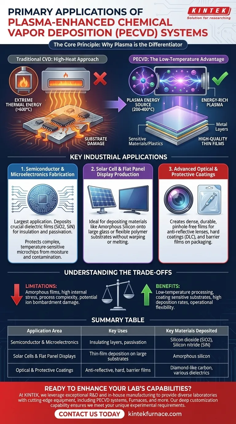
The Core Principle: Why Plasma is the Differentiator
To understand PECVD's applications, you must first understand its fundamental advantage over traditional Chemical Vapor Deposition (CVD). The difference lies in the source of energy.
Traditional CVD: The High-Heat Approach
Conventional CVD processes are like a high-temperature oven. They rely on extreme thermal energy (often >600°C) to break down precursor gases and force a chemical reaction, depositing a solid film onto a substrate.
This works well for robust materials, but it is destructive to substrates that contain plastics, previously deposited metal layers, or other temperature-sensitive components.
PECVD: The Low-Temperature Advantage
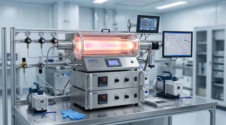
PECVD solves this problem by using plasma—an ionized gas—to supply the necessary energy. An electrical field energizes the precursor gases, creating a plasma where reactive ions and radicals are formed.
These energized particles then react and deposit on the substrate surface. Because the energy is transferred directly to the gas molecules rather than by heating the entire chamber, the substrate can be kept at a much lower temperature (typically 200-400°C).
Key Industrial Applications in Detail
This low-temperature capability is precisely why PECVD is indispensable across several key industries. It enables processes that would otherwise be impossible.
Semiconductor and Microelectronics Fabrication
This is the largest and most critical application of PECVD. Modern microchips are incredibly complex, with dozens of layers built on top of each other.
PECVD is used to deposit crucial dielectric films like silicon dioxide (SiO2) and silicon nitride (SiN). These films act as insulators between conductive layers or as a final passivation layer to protect the chip from moisture and contamination. Using a low-temperature process prevents damage to the intricate metallic circuitry already present on the wafer.
Solar Cell and Flat Panel Display Production
The production of thin-film solar cells and flat-panel displays often involves depositing materials like amorphous silicon onto large glass or flexible polymer substrates.
These substrates cannot withstand the high temperatures of traditional CVD. PECVD is the ideal method for depositing uniform silicon layers over large areas without warping or melting the underlying material.
Advanced Optical and Protective Coatings
PECVD excels at creating dense, durable, and pinhole-free films that alter surface properties.
This includes optical coatings like anti-reflective layers on lenses, hard coatings (e.g., diamond-like carbon) to make tools and mechanical parts wear-resistant, and barrier films on plastic packaging to prevent oxygen and moisture from spoiling food or medical products.
Understanding the Trade-offs
While powerful, PECVD is not a universal solution. An objective assessment requires understanding its limitations.
Film Quality and Stress
Because deposition occurs at lower temperatures, PECVD films are often amorphous (non-crystalline) or contain significant amounts of hydrogen. This can be desirable for some applications (like solar cells) but is a limitation if a highly ordered crystalline structure is required. The films can also have high internal stress, which may be a concern for some devices.
Process Complexity and Contamination
Plasma chemistry is highly complex and sensitive to parameters like pressure, power, and gas flow. Maintaining process consistency requires sophisticated control systems. Furthermore, the plasma can sputter material from the chamber walls, which can become a source of contamination if not properly managed.
Potential for Substrate Damage
Although the overall temperature is low, the substrate is exposed to bombardment by energetic ions from the plasma. This can cause minor surface damage, which may be a factor for extremely sensitive electronic or optical device interfaces.
Making the Right Choice for Your Goal
Selecting a deposition technology depends entirely on the required film properties and the limitations of your substrate.
- If your primary focus is processing temperature-sensitive substrates: PECVD is almost always the superior choice for depositing high-quality dielectric or protective films without damaging underlying components.
- If your primary focus is achieving the highest possible film purity and crystallinity: High-temperature methods like Low-Pressure CVD (LPCVD) or epitaxial growth may be necessary, provided your substrate can tolerate the heat.
- If your primary focus is creating dense, uniform protective layers at high deposition rates: PECVD offers an excellent balance of film quality, process speed, and operational flexibility for a wide range of materials.
Ultimately, PECVD's strategic value comes from its ability to separate the deposition reaction from the need for high heat, opening up a world of possibilities for advanced material fabrication.
Summary Table:
| Application Area | Key Uses | Key Materials Deposited |
|---|---|---|
| Semiconductor & Microelectronics | Insulating layers, passivation | Silicon dioxide (SiO2), Silicon nitride (SiN) |
| Solar Cells & Flat Panel Displays | Thin-film deposition on large substrates | Amorphous silicon |
| Optical & Protective Coatings | Anti-reflective, hard, barrier films | Diamond-like carbon, various dielectrics |
Ready to enhance your lab's capabilities with advanced high-temperature furnace solutions? At KINTEK, we leverage exceptional R&D and in-house manufacturing to provide diverse laboratories with cutting-edge equipment, including PECVD systems, Muffle, Tube, Rotary Furnaces, Vacuum & Atmosphere Furnaces, and more. Our strong deep customization capability ensures we can precisely meet your unique experimental requirements, helping you achieve superior thin film deposition and material processing. Contact us today to discuss how our solutions can drive your innovations forward!
Visual Guide
Related Products
- RF PECVD System Radio Frequency Plasma Enhanced Chemical Vapor Deposition
- Slide PECVD Tube Furnace with Liquid Gasifier PECVD Machine
- Inclined Rotary Plasma Enhanced Chemical Deposition PECVD Tube Furnace Machine
- Inclined Rotary Plasma Enhanced Chemical Deposition PECVD Tube Furnace Machine
- 915MHz MPCVD Diamond Machine Microwave Plasma Chemical Vapor Deposition System Reactor
People Also Ask
- How is silicon dioxide deposited from tetraethylorthosilicate (TEOS) in PECVD? Achieve Low-Temperature, High-Quality SiO2 Films
- What is the role of RF power in PECVD and how does the RF-PECVD process work? Master Thin Film Deposition Control
- What are the key advantages of PECVD technology? Achieve Low-Temperature, High-Quality Thin Film Deposition
- What are the advantages of PECVD in film deposition? Achieve Low-Temp, High-Quality Coatings
- How are deposition rates and film properties controlled in PECVD? Master Key Parameters for Optimal Thin Films


