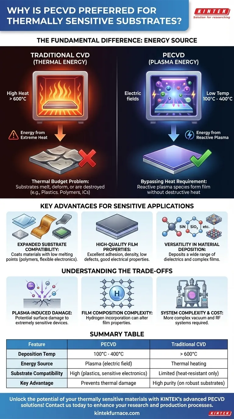
At its core, Plasma-Enhanced Chemical Vapor Deposition (PECVD) is the preferred method for thermally sensitive substrates because it replaces the intense heat required by traditional CVD with energy from a plasma. This fundamental shift allows for the deposition of high-quality thin films at significantly lower temperatures, typically between 100°C and 400°C, thereby preventing damage to materials that cannot withstand high thermal loads.
The critical insight is that PECVD decouples the energy source for chemical reactions from the substrate's temperature. Instead of heating the entire system to break down precursor gases, it uses an electric field to create a reactive plasma, enabling film growth without subjecting the substrate to destructive heat.
The Fundamental Difference: Thermal vs. Plasma Energy
The choice between PECVD and conventional CVD hinges on how energy is supplied to the chemical precursors. This single difference has profound implications for the types of materials you can work with.
Traditional CVD: The Thermal Budget Problem
Conventional Chemical Vapor Deposition (CVD) relies exclusively on thermal energy. The substrate and precursor gases are heated to very high temperatures, often exceeding 600°C.
This high heat provides the activation energy needed for the gases to react and deposit a solid film onto the substrate. This "thermal budget" is simply too high for many materials, such as plastics, polymers, and certain integrated circuits, which would melt, deform, or be destroyed.
PECVD: Bypassing the Heat Requirement
PECVD introduces a new form of energy into the equation: plasma. A plasma is a highly energized state of gas created by applying a strong electric field.
This process strips electrons from the gas atoms, creating a mixture of highly reactive ions, radicals, and free electrons.
How Plasma Enables Low-Temperature Deposition
The key is that the reactive species within the plasma already possess the energy needed to react and form the desired film. They don't need additional energy from a hot surface.
When these energetic particles come into contact with the comparatively cool substrate, they condense and form a high-quality, dense film. The energy for the reaction comes from the plasma itself, not from heating the substrate to extreme temperatures.
Key Advantages for Sensitive Applications
The low-temperature nature of PECVD unlocks capabilities that are impossible with high-heat methods, making it indispensable for modern electronics and materials science.
Expanded Substrate Compatibility
The most direct benefit is the ability to coat materials with low melting points or thermal stability. This dramatically expands the range of viable substrates.
This includes polymers, flexible plastics, and complex electronic devices with pre-existing components that cannot tolerate high-temperature processing.
High-Quality Film Properties
Despite the low temperature, PECVD produces films with excellent characteristics. The energetic plasma environment promotes strong substrate adhesion.
Furthermore, it can create films with excellent density, low defect rates, and good electrical properties (like insulation or conductivity), which are critical for high-performance devices.
Versatility in Material Deposition
The plasma-driven process is highly versatile, allowing for the deposition of a wider range of materials than many traditional CVD methods.
This includes common dielectrics like silicon nitride (SiN) and silicon dioxide (SiO₂), as well as more complex films used in semiconductor manufacturing and protective coatings.
Understanding the Trade-offs
While powerful, PECVD is not a universal solution. An objective assessment requires understanding its potential downsides.
Potential for Plasma-Induced Damage
The same high-energy ions that enable low-temperature deposition can also physically bombard the substrate surface. For extremely sensitive electronic devices, this can introduce subtle surface or subsurface damage.
Film Composition Complexity
Because precursor gases often contain hydrogen (e.g., in silane, SiH₄), PECVD films can incorporate hydrogen atoms into their structure. This can alter the film's electrical and mechanical properties and must be carefully controlled during the process.
System Complexity
PECVD reactors are inherently more complex and expensive than simple thermal CVD furnaces. They require sophisticated vacuum systems, gas handling, and radio-frequency (RF) power supplies to generate and sustain the plasma.
Making the Right Choice for Your Goal
Your choice of deposition technology must be aligned with your substrate's limitations and your desired film properties.
- If your primary focus is coating heat-sensitive materials like plastics or polymers: PECVD is the definitive and often only choice due to its low-temperature process.
- If your primary focus is achieving the highest possible film purity and crystallinity on a robust substrate: A high-temperature thermal CVD process may be superior, provided your substrate can easily withstand the heat.
- If your primary focus is balancing device performance and substrate flexibility: PECVD offers an outstanding compromise, enabling high-quality coatings for advanced applications on a vast range of materials.
Ultimately, understanding how PECVD uses plasma to replace heat empowers you to leverage its unique advantages for innovative material and device fabrication.
Summary Table:
| Feature | PECVD | Traditional CVD |
|---|---|---|
| Deposition Temperature | 100°C - 400°C | > 600°C |
| Energy Source | Plasma (electric field) | Thermal heating |
| Substrate Compatibility | High (plastics, polymers, sensitive electronics) | Limited (heat-resistant materials only) |
| Film Quality | High adhesion, density, and versatility | High purity, but requires high heat |
| Key Advantage | Prevents thermal damage to substrates | Suitable for robust substrates |
Unlock the potential of your thermally sensitive materials with KINTEK's advanced PECVD solutions! Leveraging exceptional R&D and in-house manufacturing, we provide diverse laboratories with high-temperature furnace systems like our CVD/PECVD Systems, designed for precise, low-temperature deposition. Our strong deep customization capability ensures we meet your unique experimental needs, protecting substrates while delivering high-quality thin films. Contact us today to discuss how we can enhance your research and production processes!
Visual Guide
Related Products
- RF PECVD System Radio Frequency Plasma Enhanced Chemical Vapor Deposition
- Slide PECVD Tube Furnace with Liquid Gasifier PECVD Machine
- Inclined Rotary Plasma Enhanced Chemical Deposition PECVD Tube Furnace Machine
- Inclined Rotary Plasma Enhanced Chemical Deposition PECVD Tube Furnace Machine
- Cylindrical Resonator MPCVD Machine System for Lab Diamond Growth
People Also Ask
- How are deposition rates and film properties controlled in PECVD? Master Key Parameters for Optimal Thin Films
- How does film quality compare between PECVD and CVD? Choose the Best Method for Your Substrate
- What is PECVD specification? A Guide to Choosing the Right System for Your Lab
- What are the key advantages of PECVD technology? Achieve Low-Temperature, High-Quality Thin Film Deposition
- What is the role of RF power in PECVD and how does the RF-PECVD process work? Master Thin Film Deposition Control


