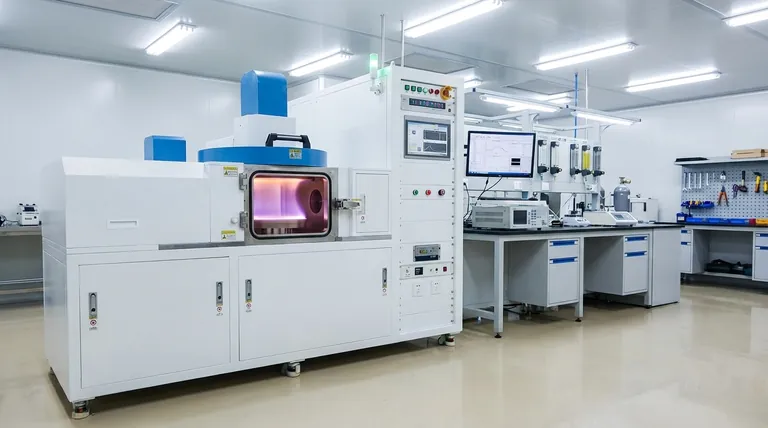
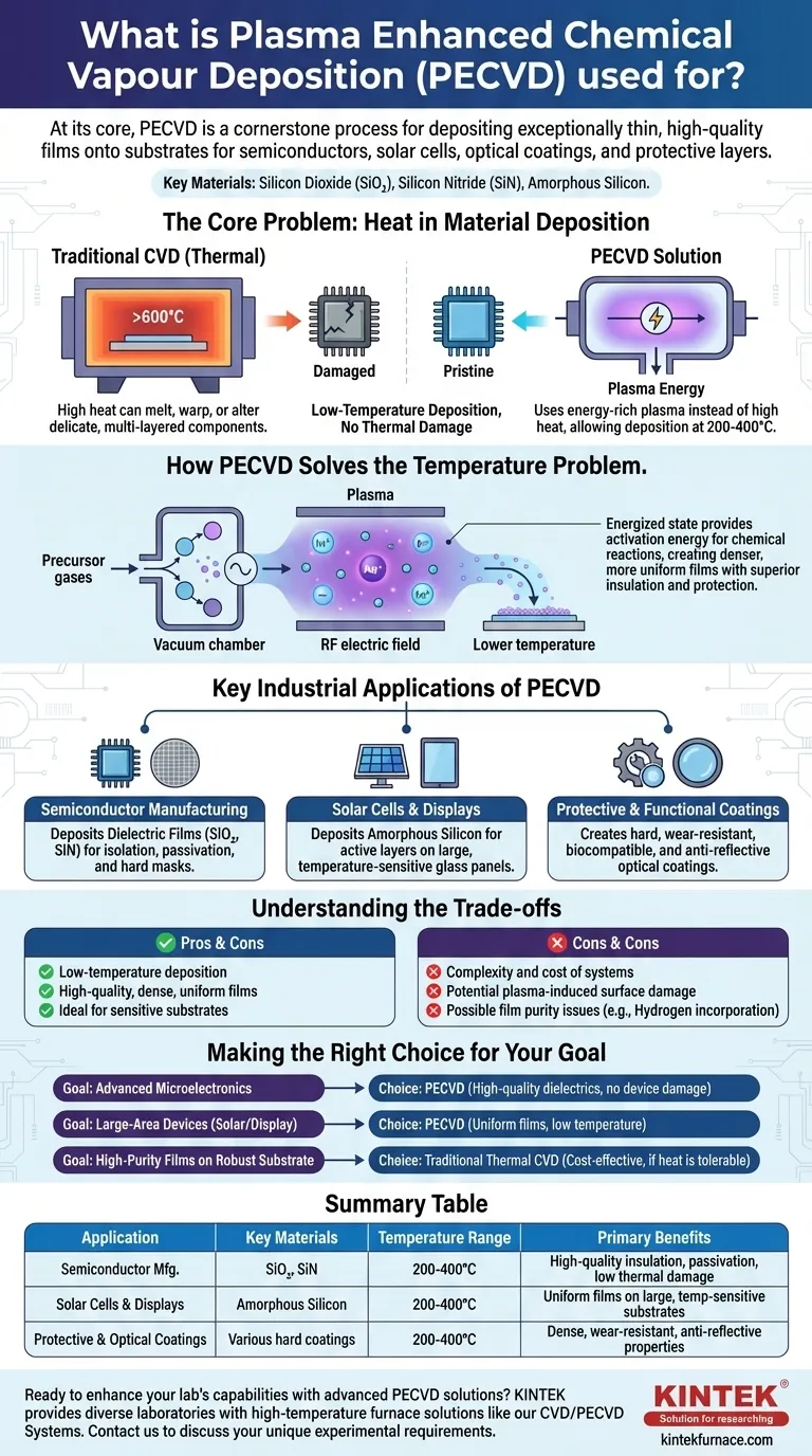
At its core, Plasma Enhanced Chemical Vapor Deposition (PECVD) is a cornerstone process used to deposit exceptionally thin, high-quality films onto a substrate. It is indispensable in high-tech manufacturing, serving critical roles in the production of semiconductors, solar cells, optical coatings, and protective layers for advanced materials. PECVD is specifically used to create materials like silicon dioxide, silicon nitride, and amorphous silicon that function as insulators, protective barriers, or active electronic layers.
The fundamental challenge in modern device fabrication is depositing a perfect film without damaging the delicate, multi-layered components already on the substrate. PECVD's primary advantage is its use of an energy-rich plasma instead of high heat, allowing for high-quality film deposition at significantly lower temperatures than traditional methods.
The Core Problem: Heat in Material Deposition
To understand the value of PECVD, we must first understand the limitations of its predecessor, thermal Chemical Vapor Deposition (CVD).
How Traditional CVD Works
In a thermal CVD process, a substrate is placed in a high-temperature furnace. Precursor gases are introduced, and the intense heat breaks them down, causing a chemical reaction that deposits a solid thin film onto the substrate surface.
The Damage Caused by High Temperatures
This process works well for robust, single-material substrates. However, in complex microelectronics, the substrate already contains intricate, fragile transistor structures. The high temperatures of thermal CVD (often >600°C) can melt, warp, or alter the electrical properties of these pre-existing layers, destroying the device.
How PECVD Solves the Temperature Problem
PECVD was developed specifically to overcome this thermal limitation. It re-engineers the deposition process by changing the source of energy.
Introducing Plasma as an Energy Source
Instead of relying solely on heat, PECVD uses an electric field to ionize the precursor gases, creating a plasma. This plasma is an energized state of matter containing highly reactive ions and free radicals.
The Benefit: Low-Temperature Deposition
This energetic plasma provides the activation energy needed for the chemical reactions to occur, dramatically reducing the required substrate temperature (typically to 200-400°C). This allows for deposition on fully fabricated wafers with sensitive components, as well as on low-cost, temperature-sensitive substrates like glass or plastic.
The Result: High-Performance Films
The plasma-driven process also leads to faster reaction kinetics and helps create denser, more uniform films. This results in superior electrical insulation, better protection against moisture and contaminants (passivation), and improved optical properties.
Key Industrial Applications of PECVD
PECVD's low-temperature advantage makes it the go-to process for numerous applications where thermal budget is a primary concern.
In Semiconductor Manufacturing
PECVD is used to deposit dielectric films (insulators) like silicon nitride (SiN) and silicon dioxide (SiO₂). These layers are critical for isolating conductive lines, passivating the final chip to protect it from the environment, and serving as hard masks for etching patterns.
For Solar Cells and Displays
The process is essential for depositing amorphous silicon films, which are the active semiconductor layer in many thin-film solar cells. Because these are often built on large glass panels, the lower temperature of PECVD is a necessity.
For Protective and Functional Coatings
PECVD creates hard, wear-resistant coatings on tools, biocompatible barrier coatings on medical implants, and anti-reflective optical coatings on lenses. Its ability to create dense films at low temperatures is key to these applications.
Understanding the Trade-offs
While powerful, PECVD is not a universal solution. Acknowledging its limitations is crucial for making an informed technical decision.
Complexity and Cost
PECVD systems, with their required RF power generators and vacuum technology, are more complex and expensive to purchase and maintain than simpler thermal CVD furnaces.
Potential for Plasma-Induced Damage
The high-energy ions within the plasma can, if not properly controlled, physically bombard and damage the substrate surface. Optimizing the plasma chemistry and energy is a critical engineering challenge.
Film Purity
Because the precursor gases are not fully broken down as they might be at higher temperatures, PECVD films can sometimes incorporate contaminants like hydrogen. This can impact the film's electrical performance in certain sensitive applications.
Making the Right Choice for Your Goal
Selecting a deposition method depends entirely on the thermal budget of your substrate and the required film properties.
- If your primary focus is fabricating advanced microelectronics: PECVD is the default choice for depositing high-quality dielectric layers without damaging underlying device structures.
- If your primary focus is large-area devices like solar panels or displays: PECVD's ability to deposit uniform films over large, temperature-sensitive substrates makes it the enabling technology.
- If your primary focus is high-purity films on a robust substrate: Traditional high-temperature thermal CVD may be a more cost-effective and simpler option, provided your substrate can tolerate the heat.
Ultimately, understanding the trade-off between thermal energy and plasma energy is the key to selecting the ideal deposition technology for your specific engineering goal.
Summary Table:
| Application | Key Materials Deposited | Temperature Range | Primary Benefits |
|---|---|---|---|
| Semiconductor Manufacturing | Silicon Dioxide (SiO₂), Silicon Nitride (SiN) | 200-400°C | High-quality insulation, passivation, low thermal damage |
| Solar Cells & Displays | Amorphous Silicon | 200-400°C | Uniform films on large, temperature-sensitive substrates |
| Protective & Optical Coatings | Various hard coatings, barrier layers | 200-400°C | Dense, wear-resistant, and anti-reflective properties |
Ready to enhance your lab's capabilities with advanced PECVD solutions? Leveraging exceptional R&D and in-house manufacturing, KINTEK provides diverse laboratories with high-temperature furnace solutions like our CVD/PECVD Systems. Our strong deep customization capability ensures we precisely meet your unique experimental requirements for low-temperature film deposition. Contact us today to discuss how we can support your projects in semiconductors, solar cells, and coatings!
Visual Guide
Related Products
- RF PECVD System Radio Frequency Plasma Enhanced Chemical Vapor Deposition
- Slide PECVD Tube Furnace with Liquid Gasifier PECVD Machine
- Inclined Rotary Plasma Enhanced Chemical Deposition PECVD Tube Furnace Machine
- Inclined Rotary Plasma Enhanced Chemical Deposition PECVD Tube Furnace Machine
- MPCVD Machine System Reactor Bell-jar Resonator for Lab and Diamond Growth
People Also Ask
- What are the key advantages of PECVD technology? Achieve Low-Temperature, High-Quality Thin Film Deposition
- What is RF in PECVD? A Critical Control for Plasma Deposition
- What are some promising applications of PECVD-prepared 2D materials? Unlock Advanced Sensing and Optoelectronics
- What is the role of RF power in PECVD and how does the RF-PECVD process work? Master Thin Film Deposition Control
- What are the advantages of PECVD in film deposition? Achieve Low-Temp, High-Quality Coatings


