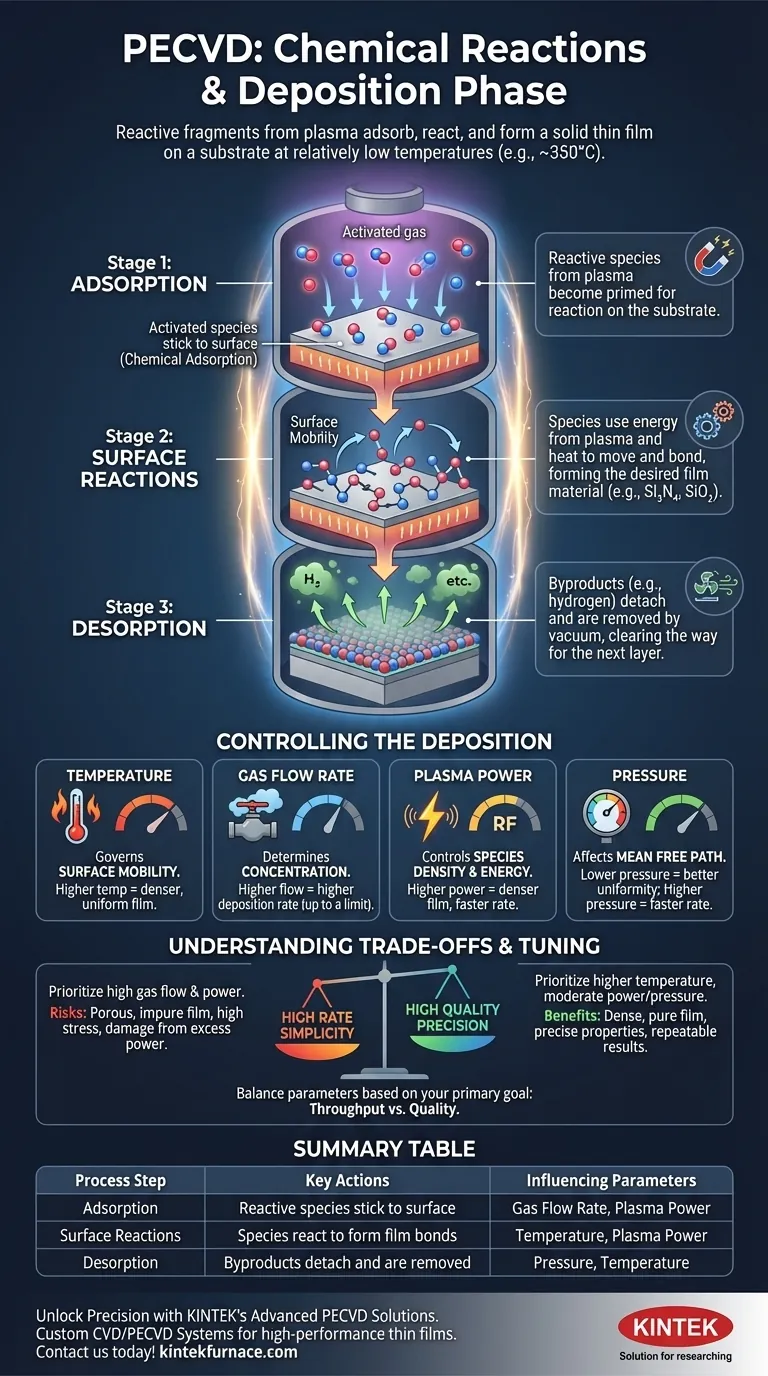
During the final phase of Plasma-Enhanced Chemical Vapor Deposition (PECVD), reactive chemical fragments created by the plasma adsorb onto the substrate surface. There, they undergo a series of chemical reactions to form the solid thin film, while waste byproducts are released. This entire process is accomplished at relatively low temperatures, often around 350°C, distinguishing it from higher-temperature deposition methods.
PECVD's deposition phase is not a simple "splattering" of material. It is a controlled, three-step surface chemistry process—adsorption, reaction, and desorption—where the final film's quality is directly manipulated by tuning external process parameters like power, temperature, and gas flow.
The Core Mechanism: From Gas to Solid Film
To understand deposition in PECVD, it's best to break it down into a sequence of events occurring directly on the substrate surface. This surface chemistry is what ultimately builds your film, one molecular layer at a time.
Step 1: Adsorption of Reactive Species
The plasma phase creates highly reactive molecules and atoms from the precursor gases. These activated species then travel and stick to the substrate surface in a process called chemical adsorption. They are now primed for reaction but are not yet the final film material.
Step 2: Surface Reactions and Film Formation
Once adsorbed, the species have enough energy—provided by the plasma and the heated substrate—to move around slightly (surface mobility) and react with each other. These surface reactions form the chemical bonds of the desired thin-film material, such as silicon nitride (Si₃N₄) or silicon dioxide (SiO₂).
Step 3: Desorption of Byproducts
The chemical reactions that form the film also create unwanted byproducts (e.g., hydrogen gas). For a dense, pure film to grow, these byproducts must detach from the surface and be removed by the vacuum system. This final step, desorption, clears the way for the next layer of reactive species to adsorb.
How Process Parameters Control Deposition
The quality, thickness, and properties of the deposited film are not accidental. They are the direct result of carefully controlling four key process parameters that influence the surface reactions.
The Role of Temperature
While PECVD is a "low-temperature" process, the substrate temperature is critical. It governs the surface mobility of the adsorbed species. Higher temperatures give the atoms more energy to move into ideal positions, resulting in a denser, more uniform, and less stressed film.
The Impact of Gas Flow Rate
The gas flow rate determines the concentration of reactant species available in the chamber. Increasing the flow rate can increase the deposition rate, as more raw material is supplied to the surface. However, there is a limit where too much flow can disrupt the plasma's stability.
The Influence of Plasma Power
RF plasma power controls the density and energy of the reactive species. Higher power creates more fragments and imparts more energy, which can lead to a denser film and a faster deposition rate. This energy helps drive the surface reactions.
The Function of Pressure
Chamber pressure affects the "mean free path" of the gas molecules—the average distance they travel before colliding. Lower pressure leads to a longer mean free path, which can improve film uniformity across the substrate. Conversely, higher pressure can increase the deposition rate by concentrating reactants near the surface.
Understanding the Trade-offs
Achieving the perfect film requires balancing competing factors. Adjusting one parameter to improve a single property can often negatively affect another.
Rate vs. Quality
Pushing for the highest possible deposition rate by increasing gas flow and power can be detrimental. These conditions can lead to a more porous, impure, or highly stressed film because the surface reactions become too frantic, and byproducts don't have enough time to desorb properly.
Energy vs. Damage
While plasma energy is necessary to drive reactions, excessive power can cause damage. High-energy ion bombardment can create defects in the growing film or even damage the underlying substrate, which is especially critical when working with sensitive electronic devices.
Uniformity vs. Simplicity
Achieving a perfectly uniform film thickness and consistent material properties across a large wafer is a significant challenge. It requires complex showerhead designs for gas delivery and meticulous tuning of pressure and plasma fields, adding complexity to the process.
Tuning the Process for Your Goal
The optimal parameters depend entirely on what you want to achieve with your thin film. Your "best" process is defined by your primary objective.
- If your primary focus is high throughput: Prioritize increasing gas flow rates and plasma power to maximize the deposition rate, but be prepared to monitor and accept potential compromises in film stress and density.
- If your primary focus is superior film quality (density and purity): Use a slightly higher substrate temperature to enhance surface mobility and moderate plasma power to ensure complete reactions without causing damage.
- If your primary focus is precise material properties (e.g., refractive index): Focus on meticulously controlling the ratio of precursor gases and use stable, moderate power and pressure settings to ensure repeatable chemical incorporation.
Ultimately, mastering the PECVD deposition phase is about understanding how to manipulate these external controls to precisely engineer the film's final structure and performance.
Summary Table:
| Process Step | Key Actions | Influencing Parameters |
|---|---|---|
| Adsorption | Reactive species stick to substrate surface | Gas flow rate, Plasma power |
| Surface Reactions | Species react to form film bonds | Temperature, Plasma power |
| Desorption | Byproducts detach and are removed | Pressure, Temperature |
Unlock Precision in Your Laboratory with KINTEK's Advanced PECVD Solutions
Leveraging exceptional R&D and in-house manufacturing, KINTEK provides diverse laboratories with advanced high-temperature furnace solutions, including our specialized CVD/PECVD Systems. Our strong deep customization capability ensures we can precisely meet your unique experimental requirements, delivering reliable, high-performance thin films for applications in electronics, optics, and more.
Ready to enhance your deposition processes? Contact us today to discuss how our tailored PECVD systems can optimize your research and production outcomes!
Visual Guide
Related Products
- RF PECVD System Radio Frequency Plasma Enhanced Chemical Vapor Deposition
- Slide PECVD Tube Furnace with Liquid Gasifier PECVD Machine
- Inclined Rotary Plasma Enhanced Chemical Deposition PECVD Tube Furnace Machine
- Inclined Rotary Plasma Enhanced Chemical Deposition PECVD Tube Furnace Machine
- Cylindrical Resonator MPCVD Machine System for Lab Diamond Growth
People Also Ask
- What are the advantages of PECVD in film deposition? Achieve Low-Temp, High-Quality Coatings
- What is RF in PECVD? A Critical Control for Plasma Deposition
- What is PECVD specification? A Guide to Choosing the Right System for Your Lab
- How is silicon dioxide deposited from tetraethylorthosilicate (TEOS) in PECVD? Achieve Low-Temperature, High-Quality SiO2 Films
- What is the role of RF power in PECVD and how does the RF-PECVD process work? Master Thin Film Deposition Control


