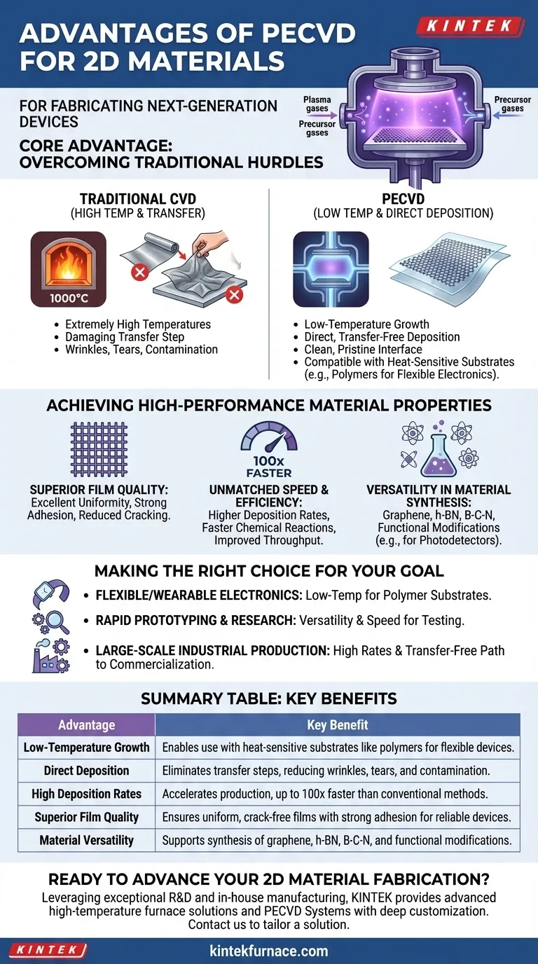
For fabricating next-generation devices, Plasma-Enhanced Chemical Vapor Deposition (PECVD) stands out as a superior method for preparing 2D materials. Its primary advantages are the ability to operate at low temperatures and deposit materials directly onto a final substrate, eliminating the damaging transfer step common to other methods. This combination enables the scalable, low-cost production of high-quality 2D materials with clean interfaces, ready for device integration.
PECVD is not just an alternative fabrication technique; it is a strategic solution to the core challenges that have historically hindered the commercialization of 2D materials. By sidestepping the high temperatures and complex transfer processes of traditional CVD, it opens a direct path to industrial-scale production.
The Core Advantage: Overcoming Traditional Hurdles
The true value of PECVD is best understood by comparing it to the limitations of conventional Chemical Vapor Deposition (CVD). PECVD was engineered to solve these specific, critical bottlenecks.
Lower Temperature Growth
Traditional CVD often requires extremely high temperatures (around 1000°C), which is incompatible with many technologically important substrates.
PECVD uses plasma to energize the precursor gases, initiating chemical reactions at much lower temperatures. This allows for deposition on heat-sensitive substrates like polymers, making it ideal for creating flexible electronics, wearable sensors, and other advanced devices.
The End of the Transfer Process
A major drawback of conventional CVD for 2D materials is the need for a separate transfer step. The material is grown on a catalytic metal foil and then must be moved to the final device substrate.
This transfer process is notorious for introducing wrinkles, tears, and contamination, which degrade the material's performance and make large-scale production unreliable. PECVD avoids this entirely by enabling direct, transfer-free deposition onto the desired non-catalytic substrate, ensuring a clean and pristine material interface.
Achieving High-Performance Material Properties
Beyond solving fundamental production issues, PECVD enables the creation of materials with superior characteristics suited for demanding applications.
Superior Film Quality and Uniformity
The plasma-driven process promotes the growth of high-quality thin films. These films exhibit excellent uniformity across the substrate, strong adhesion, and a reduced risk of cracking. This structural integrity is critical for fabricating reliable electronic and optical devices.
Unmatched Speed and Efficiency
Plasma significantly accelerates chemical reactions, leading to much higher deposition rates compared to conventional methods. For some materials, this can be over 100 times faster, dramatically improving throughput and reducing manufacturing costs, which is a key factor for industrial compatibility.
Versatility in Material Synthesis and Modification
PECVD is not limited to a single material. It is a versatile platform capable of preparing a wide variety of 2D materials, including:
- Pristine and nitrogen-doped graphene
- Hexagonal boron nitride (h-BN)
- Ternary compounds like B–C–N
Furthermore, a mild plasma process can be used to treat or functionally modify existing 2D materials (like WSe2), precisely tuning their properties for specific applications such as photodetectors, biochemical sensors, and electronic skins.
Understanding the Trade-offs and Outlook
While PECVD offers clear advantages, it is important to have a complete picture of its current status and future development.
The Need for Process Optimization
Like any advanced manufacturing technique, achieving the ideal material properties for a specific, cutting-edge application requires careful optimization. Fine-tuning parameters like gas composition, pressure, and plasma power is essential to control factors like crystal size and defect density.
Scaling from Lab to Fab
PECVD is inherently scalable and compatible with existing industrial semiconductor manufacturing tools. However, translating a specific lab-scale process to high-volume manufacturing requires significant engineering effort to ensure absolute uniformity and repeatability across large-area substrates. The fundamental capability is there, but the implementation is non-trivial.
Making the Right Choice for Your Goal
PECVD provides a powerful pathway for 2D material synthesis, but its suitability depends on your primary objective.
- If your primary focus is creating flexible or wearable electronics: PECVD is the clear choice, as its low-temperature process is compatible with the polymer substrates these devices require.
- If your primary focus is rapid prototyping and research: The versatility and speed of PECVD allow you to quickly synthesize and test different materials and device structures.
- If your primary focus is large-scale industrial production: PECVD provides the most viable path to commercialization due to its high deposition rates, industrial compatibility, and elimination of the problematic transfer step.
Ultimately, PECVD provides a powerful and practical toolkit for translating the promise of 2D materials into functional, real-world devices.
Summary Table:
| Advantage | Key Benefit |
|---|---|
| Low-Temperature Growth | Enables use with heat-sensitive substrates like polymers for flexible devices |
| Direct Deposition | Eliminates transfer steps, reducing wrinkles, tears, and contamination |
| High Deposition Rates | Accelerates production, up to 100x faster than conventional methods |
| Superior Film Quality | Ensures uniform, crack-free films with strong adhesion for reliable devices |
| Material Versatility | Supports synthesis of graphene, h-BN, B-C-N, and functional modifications |
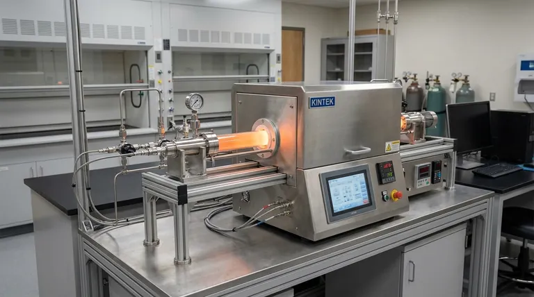
Ready to advance your 2D material fabrication? Leveraging exceptional R&D and in-house manufacturing, KINTEK provides diverse laboratories with advanced high-temperature furnace solutions. Our product line, including Muffle, Tube, Rotary Furnaces, Vacuum & Atmosphere Furnaces, and CVD/PECVD Systems, is complemented by our strong deep customization capability to precisely meet unique experimental requirements. Whether you're developing flexible electronics, wearable sensors, or scaling up production, our PECVD systems offer low-temperature, transfer-free deposition for high-quality results. Contact us today to discuss how we can tailor a solution for your needs!
Visual Guide
Related Products
- RF PECVD System Radio Frequency Plasma Enhanced Chemical Vapor Deposition
- Slide PECVD Tube Furnace with Liquid Gasifier PECVD Machine
- Inclined Rotary Plasma Enhanced Chemical Deposition PECVD Tube Furnace Machine
- Inclined Rotary Plasma Enhanced Chemical Deposition PECVD Tube Furnace Machine
- Cylindrical Resonator MPCVD Machine System for Lab Diamond Growth
People Also Ask
- What is PECVD specification? A Guide to Choosing the Right System for Your Lab
- How is silicon dioxide deposited from tetraethylorthosilicate (TEOS) in PECVD? Achieve Low-Temperature, High-Quality SiO2 Films
- What are the applications of plasma enhanced chemical vapor deposition? Key Uses in Electronics, Optics & Materials
- What are some promising applications of PECVD-prepared 2D materials? Unlock Advanced Sensing and Optoelectronics
- What are the advantages of PECVD in film deposition? Achieve Low-Temp, High-Quality Coatings


