At its core, the primary advantage of Plasma-Enhanced Chemical Vapor Deposition (PECVD) over traditional thermal CVD is its ability to operate at significantly lower temperatures. This is achieved by using plasma to energize the chemical reaction instead of high heat, which unlocks the ability to coat thermally sensitive substrates while often achieving higher deposition rates and more uniform films.
The fundamental difference is the energy source. Thermal CVD uses intense heat to break down precursor gases, while PECVD uses an energy-efficient plasma. This decouples the deposition process from high temperatures, making it a more versatile and often more cost-effective solution for modern materials.
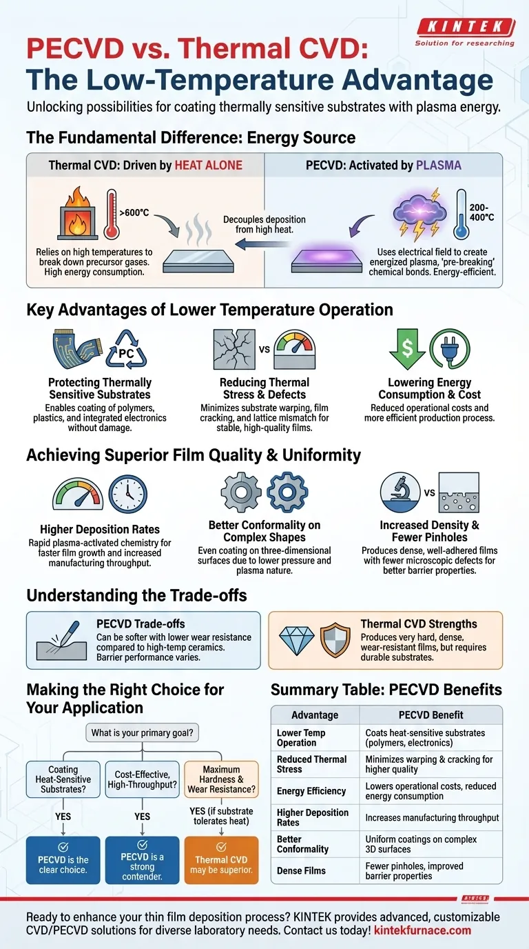
The Fundamental Difference: Energy Source
To understand the advantages of PECVD, you must first understand how it differs from thermal CVD at a process level. The choice of energy source dictates the capabilities and limitations of each method.
Thermal CVD: Driven by Heat Alone
Traditional thermal CVD relies exclusively on high temperatures, often exceeding 600°C, to provide the necessary activation energy. This heat forces the precursor gases to decompose and react on the substrate surface, forming the desired thin film.
PECVD: Activated by Plasma
PECVD introduces an electrical field to create a plasma, a highly energized state of matter. This plasma effectively "pre-breaks" the chemical bonds in the precursor gases at a much lower bulk temperature (typically 200-400°C), creating highly reactive species that then deposit onto the substrate.
Key Advantages of Lower Temperature Operation
The ability to operate at low temperatures is not just an incremental improvement; it is a transformative capability that fundamentally changes what is possible in thin film deposition.
Protecting Thermally Sensitive Substrates
This is the most significant advantage of PECVD. Materials like polymers, plastics, and many integrated electronic devices cannot withstand the extreme heat of thermal CVD. PECVD makes it possible to deposit high-quality films on these temperature-sensitive substrates without damaging or destroying them.
Reducing Thermal Stress and Defects
High temperatures create thermal stress, which can cause the substrate to warp or the deposited film to crack upon cooling. This temperature difference can also lead to lattice mismatch between the substrate and the film, introducing defects. PECVD's low-temperature process dramatically minimizes these issues, resulting in more stable, higher-quality films.
Lowering Energy Consumption and Cost
Heating a reaction chamber to the high temperatures required by thermal CVD consumes a significant amount of energy. By operating at lower temperatures, PECVD reduces energy consumption, leading to lower operational costs and a more efficient production process.
Achieving Superior Film Quality and Uniformity
Beyond temperature, PECVD offers distinct advantages in the quality and consistency of the final film, especially on complex geometries.
Higher Deposition Rates
In many cases, the plasma-activated chemistry of PECVD can proceed more rapidly than thermally-driven reactions. This allows for faster film growth, increasing manufacturing throughput.
Better Conformality on Complex Shapes
PECVD typically operates at lower pressures than atmospheric pressure CVD. This, combined with the nature of the plasma, allows the reactive gas species to coat complex, three-dimensional surfaces more evenly, resulting in a more uniform and conformal coating.
Increased Density and Fewer Pinholes
The lower process temperature helps produce films that are dense, well-adhered, and have fewer microscopic defects like pinholes. This is critical for applications requiring strong barrier properties or electrical insulation.
Understanding the Trade-offs
No technology is without limitations. While powerful, PECVD is not a universal solution, and its films have different properties than those produced by high-temperature methods.
Film Hardness and Wear Resistance
Because PECVD films are deposited at lower temperatures, they can be softer and have lower wear resistance compared to the very hard, dense ceramic films often produced by high-temperature thermal CVD.
Barrier Performance
While PECVD films are dense, their barrier performance against moisture or gases can sometimes be weaker than specialized polymers like Parylene or films deposited under different conditions. The final performance is highly dependent on the specific precursors and plasma parameters used.
Process Complexity and Contaminants
The use of plasma introduces additional process variables that must be controlled. Furthermore, some precursor gases, particularly halogenated ones, can pose environmental or health concerns if not handled properly.
Making the Right Choice for Your Application
The decision between PECVD and thermal CVD depends entirely on your substrate material and the desired properties of the final film.
- If your primary focus is coating heat-sensitive substrates (like polymers or electronics): PECVD is the clear and often only choice due to its low-temperature process.
- If your primary focus is achieving maximum hardness and wear resistance on a durable substrate: High-temperature thermal CVD may produce a superior film, provided the substrate can tolerate the intense heat.
- If your primary focus is cost-effective, high-throughput manufacturing of uniform films: PECVD is a strong contender due to its higher deposition rates and lower energy requirements.
Ultimately, selecting the right deposition technology requires a clear understanding of your specific engineering goals and material constraints.
Summary Table:
| Advantage | PECVD Benefit |
|---|---|
| Lower Temperature Operation | Enables coating of heat-sensitive substrates like polymers and electronics |
| Reduced Thermal Stress | Minimizes substrate warping and film cracking for higher quality |
| Energy Efficiency | Lowers operational costs with reduced energy consumption |
| Higher Deposition Rates | Increases manufacturing throughput with faster film growth |
| Better Conformality | Provides uniform coatings on complex 3D surfaces |
| Dense Films | Results in fewer pinholes and improved barrier properties |
Ready to enhance your thin film deposition process? Leveraging exceptional R&D and in-house manufacturing, KINTEK provides diverse laboratories with advanced high-temperature furnace solutions. Our product line, including Muffle, Tube, Rotary Furnaces, Vacuum & Atmosphere Furnaces, and CVD/PECVD Systems, is complemented by our strong deep customization capability to precisely meet unique experimental requirements. Whether you're working with heat-sensitive substrates or need tailored CVD solutions, we can help you achieve superior results. Contact us today to discuss how our expertise can benefit your specific application!
Visual Guide
Related Products
- Slide PECVD Tube Furnace with Liquid Gasifier PECVD Machine
- RF PECVD System Radio Frequency Plasma Enhanced Chemical Vapor Deposition
- Inclined Rotary Plasma Enhanced Chemical Deposition PECVD Tube Furnace Machine
- Inclined Rotary Plasma Enhanced Chemical Deposition PECVD Tube Furnace Machine
- Multi Heating Zones CVD Tube Furnace Machine for Chemical Vapor Deposition Equipment
People Also Ask
- What are the advantages of using a tube furnace CVD system for Cu(111)/graphene? Superior Scalability and Quality
- How does a hydrogen reduction environment in an industrial tube furnace facilitate gold-copper alloy microspheres?
- In which industries is the tube furnace commonly used? Essential for Materials Science, Energy, and More
- How does PECVD equipment contribute to TOPCon bottom cells? Mastering Hydrogenation for Maximum Solar Efficiency
- What are the main advantages of PECVD tube furnaces compared to CVD tube furnaces? Lower Temp, Faster Deposition, and More


