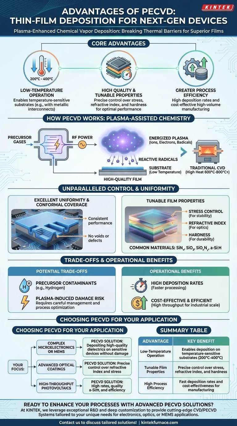
At its core, Plasma-Enhanced Chemical Vapor Deposition (PECVD) provides three primary advantages over conventional deposition methods: it operates at significantly lower temperatures, yields higher quality films with tunable properties, and offers greater process efficiency. This unique combination allows for the deposition of robust thin films on temperature-sensitive materials, a critical capability in modern electronics and optics manufacturing.
The fundamental benefit of PECVD is its use of plasma to energize precursor gases, breaking the dependence on high thermal energy. This decoupling allows for the growth of dense, high-quality films at low temperatures, enabling complex device fabrication that would otherwise be impossible.
The Fundamental Advantage: Breaking the Temperature Barrier
The most transformative characteristic of PECVD is its low-temperature operation, typically between 200°C and 400°C. This is a dramatic reduction compared to traditional Chemical Vapor Deposition (CVD), which often requires temperatures of 600°C to 800°C or higher.
How PECVD Works: Plasma-Enhanced Chemistry
Instead of relying solely on thermal energy to initiate chemical reactions, PECVD introduces energy into a chamber via an electric field, creating a plasma. This plasma is a highly energized gas containing ions, electrons, and neutral radicals.
These reactive radicals, not high heat, are what drive the deposition reaction on the substrate surface. This plasma-assisted chemistry is the key to forming high-quality films without high temperatures.
The Impact on Temperature-Sensitive Substrates
The low-temperature process is essential for building multi-layered devices. It allows for the deposition of films on top of substrates that already have metallic interconnects (like aluminum) or other structures that would be damaged or melted by high heat. This makes PECVD indispensable in semiconductor and micro-electromechanical systems (MEMS) fabrication.
Unparalleled Control Over Film Properties
Beyond temperature, PECVD provides a level of control over the final film's characteristics that is difficult to achieve with purely thermal methods. This is because process parameters like gas flow, pressure, and plasma power can be independently tuned.
Achieving High Uniformity and Conformal Coverage
PECVD is known for producing films with excellent uniformity across the entire substrate, ensuring consistent device performance. It also provides good step coverage, meaning the film conforms evenly over the microscopic topographical features of a device, preventing voids or defects.
Tuning Stress, Refractive Index, and Hardness
For applications in optics and MEMS, the physical properties of the film are critical. PECVD allows engineers to precisely control the film's internal stress, refractive index, and hardness by adjusting the deposition parameters. This control is vital for creating high-performance optical coatings and stable mechanical structures.
Depositing a Wide Range of Materials
This process is versatile and can be used to deposit a variety of crucial dielectric and semiconductor films. Common materials include high-quality silicon nitride (SiNₓ), silicon dioxide (SiO₂), silicon oxynitride (SiOₓNᵧ), and amorphous silicon (a-Si:H).
Understanding the Trade-offs and Limitations
While powerful, PECVD is not without its challenges. An objective assessment requires understanding its potential downsides compared to other methods like high-temperature thermal CVD.
The Challenge of Precursor Contaminants
Because PECVD uses precursor gases (like silane, SiH₄), films often incorporate hydrogen. While sometimes beneficial, this incorporated hydrogen can negatively impact the electrical properties of a device, a factor that must be carefully managed.
Potential for Plasma-Induced Damage
The high-energy plasma, while beneficial for the reaction, can sometimes cause physical or electrical damage to the substrate surface or underlying device layers. Optimizing the process is key to mitigating this risk.
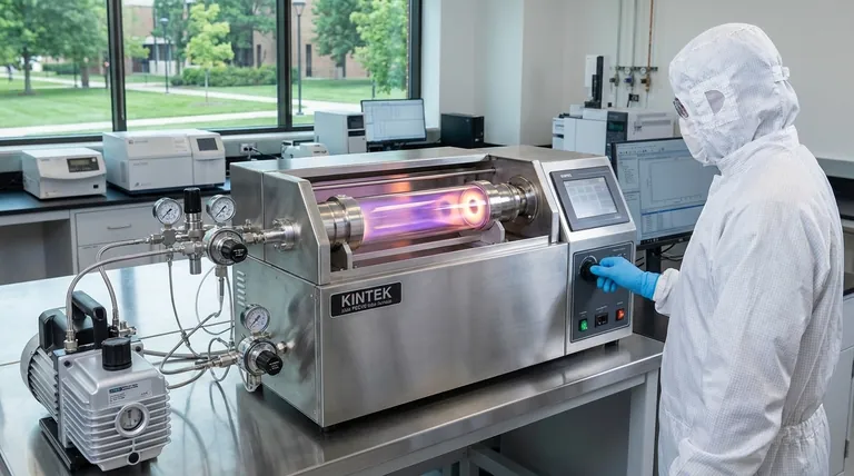
System Complexity and Cost
PECVD systems are more complex and generally have a higher capital cost than simpler thermal CVD furnaces. They require sophisticated RF power supplies, vacuum systems, and control electronics.
Key Operational Benefits
From a manufacturing perspective, PECVD offers clear advantages that contribute to its widespread adoption in high-volume production environments.
High Deposition Rates
PECVD generally achieves high deposition rates, enabling faster device processing and greater manufacturing throughput compared to some other low-temperature techniques.
Cost-Effectiveness and Efficiency
The combination of high throughput, excellent film quality, and applicability to a wide range of products makes PECVD a highly efficient and cost-effective solution for industrial-scale manufacturing, from solar cells to integrated circuits.
Making the Right Choice for Your Application
Selecting PECVD depends entirely on the specific requirements of your film and the constraints of your substrate.
- If your primary focus is fabricating complex microelectronics or MEMS: PECVD is essential for depositing high-quality dielectrics on temperature-sensitive devices without damaging underlying layers.
- If your primary focus is developing advanced optical coatings: PECVD offers the precise, independent control over refractive index and stress that is critical for meeting stringent optical performance targets.
- If your primary focus is high-throughput manufacturing of photovoltaics: The combination of high deposition rates, good material quality (especially for a-Si:H), and overall efficiency makes PECVD an industry standard.
By understanding that PECVD uses plasma to overcome thermal limitations, you can effectively leverage its advantages to build next-generation devices.
Summary Table:
| Advantage | Key Benefit |
|---|---|
| Low-Temperature Operation | Enables deposition on temperature-sensitive substrates (200°C-400°C) |
| Tunable Film Properties | Precise control over stress, refractive index, and hardness |
| High Process Efficiency | Fast deposition rates and cost-effectiveness for manufacturing |
Ready to enhance your thin-film processes with advanced PECVD solutions? At KINTEK, we leverage exceptional R&D and in-house manufacturing to provide diverse laboratories with cutting-edge high-temperature furnace systems, including our specialized CVD/PECVD Systems. Our strong deep customization capability ensures we precisely meet your unique experimental requirements, whether for electronics, optics, or MEMS applications. Contact us today to discuss how our tailored solutions can drive your innovation forward!
Visual Guide
Related Products
- Slide PECVD Tube Furnace with Liquid Gasifier PECVD Machine
- RF PECVD System Radio Frequency Plasma Enhanced Chemical Vapor Deposition
- Inclined Rotary Plasma Enhanced Chemical Deposition PECVD Tube Furnace Machine
- Inclined Rotary Plasma Enhanced Chemical Deposition PECVD Tube Furnace Machine
- Multi Heating Zones CVD Tube Furnace Machine for Chemical Vapor Deposition Equipment
People Also Ask
- What is plasma in the context of PECVD? Unlock Low-Temperature Thin Film Deposition
- What plasma source is used in PE-CVD tube furnaces? Unlock Low-Temperature, High-Quality Deposition
- How does PECVD equipment contribute to TOPCon bottom cells? Mastering Hydrogenation for Maximum Solar Efficiency
- How does a hydrogen reduction environment in an industrial tube furnace facilitate gold-copper alloy microspheres?
- What are the main advantages of PECVD tube furnaces compared to CVD tube furnaces? Lower Temp, Faster Deposition, and More


