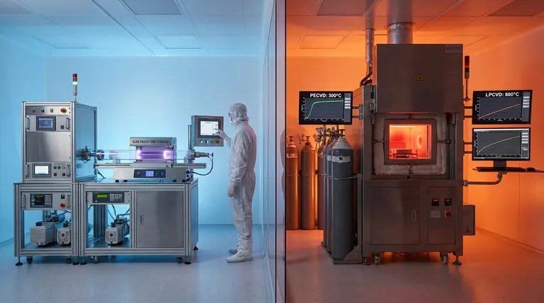
At its core, the primary advantage of Plasma-Enhanced Chemical Vapor Deposition (PECVD) over Low-Pressure Chemical Vapor Deposition (LPCVD) is its ability to operate at significantly lower temperatures. This fundamental difference allows for faster film deposition on a wider variety of materials without damaging the underlying substrate, making it indispensable for modern semiconductor fabrication and temperature-sensitive applications.
PECVD trades the high-purity, thermally-driven environment of LPCVD for a lower-temperature, plasma-assisted process. This exchange prioritizes speed and substrate versatility over the ultimate film density and purity that high-temperature processes can achieve.
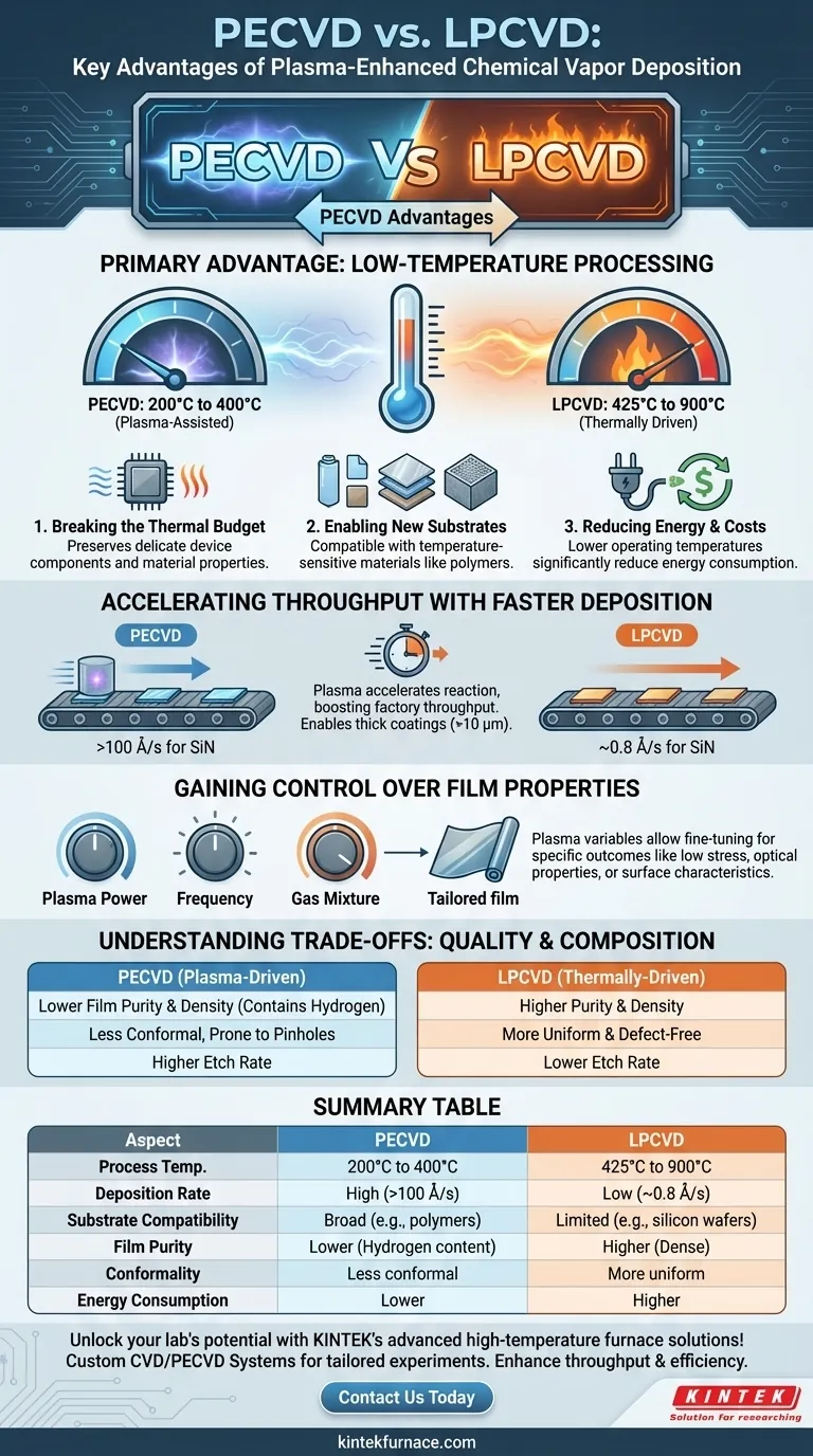
The Primary Advantage: Low-Temperature Processing
The most significant distinction between PECVD and LPCVD is the process temperature. This single factor drives most of PECVD's key benefits.
### Breaking the Thermal Budget
LPCVD is a thermally driven process, typically requiring temperatures between 425°C and 900°C to initiate the necessary chemical reactions. In contrast, PECVD uses an energetic plasma to activate the precursor gases, allowing deposition to occur at much lower temperatures, often in the 200°C to 400°C range.
As device components become smaller and more complex, this "thermal budget"—the total amount of heat a device can tolerate during manufacturing—shrinks. The low temperatures of PECVD are critical for preserving the delicate material properties and electrical characteristics of already-fabricated components on a wafer.
### Enabling New Substrates
The high heat of LPCVD limits its use to thermally robust substrates, such as silicon wafers. PECVD's gentle temperature profile makes it compatible with a vast range of temperature-sensitive materials, including polymers, plastics, and other substrates that would degrade or melt in an LPCVD reactor.
### Reducing Energy and Operational Costs
Operating a furnace at 800°C requires substantially more energy than operating one at 350°C. By lowering the process temperature, PECVD significantly reduces energy consumption, leading to lower operational costs over the lifetime of the equipment.
Accelerating Throughput with Faster Deposition
While reducing temperature is PECVD's main advantage, its ability to deposit films quickly is a close second, directly impacting production efficiency and cost.
### A Fundamental Difference in Rate
The plasma in a PECVD system dramatically accelerates the reaction and deposition process. For example, depositing silicon nitride (SiN) via PECVD at 400°C can achieve a rate of over 100 Å/second. A comparable LPCVD process at 800°C might only reach a rate of around 0.8 Å/second.
This massive increase in speed means more wafers can be processed in the same amount of time, directly boosting factory throughput.
### Enabling Thick Film Deposition
The high deposition rate also makes PECVD uniquely suited for creating thick coatings, often greater than 10 micrometers (µm). Achieving such thicknesses with the much slower LPCVD process would be impractical from a time and cost perspective.
Gaining Control Over Film Properties
The use of plasma introduces process variables that are not available in a purely thermal LPCVD system, allowing for greater control over the final film's characteristics.
### Beyond Thermal Reactions
In LPCVD, temperature and pressure are the primary control knobs. In PECVD, factors like plasma power, frequency, and gas mixture ratios provide additional levers to influence the deposition. This allows engineers to fine-tune the process to achieve specific outcomes.
### Tailoring Material Characteristics
This enhanced control allows for the creation of films with highly tailored properties. PECVD can be used to produce films with low internal stress, specific optical properties like UV protection, or desired surface characteristics like hydrophobicity.
Understanding the Trade-offs: Quality and Composition
While PECVD offers clear advantages in speed and temperature, these benefits come with inherent trade-offs, particularly regarding film purity and structure. Understanding these is critical for making an informed decision.
### Film Purity and Hydrogen Content
LPCVD films are generally of higher purity and density. The high-temperature process helps drive off impurities and creates a film that is closer to its ideal stoichiometry. PECVD films, by contrast, often have a significant amount of incorporated hydrogen from the precursor gases, which can affect the film's electrical properties and stability.
### Dealing with Pinholes and Defects
Because the deposition is so rapid and not driven by surface mobility at high temperatures, PECVD films can be less conformal and more prone to pinholes and other structural defects, especially for very thin layers (under ~4000 Å). LPCVD's slower, high-temperature process typically yields more uniform and defect-free films.
### Etch Rates and Downstream Processing
The lower density and different composition of PECVD films mean they generally have a higher etch rate than their LPCVD counterparts. This must be accounted for in subsequent manufacturing steps, as the film will be removed more quickly during plasma etching or wet chemical processes.
Making the Right Choice for Your Goal
The decision between PECVD and LPCVD is not about which is "better" overall, but which is better for a specific application.
- If your primary focus is maximum film purity and conformality on a robust substrate: LPCVD is often the superior choice due to its high-temperature, equilibrium-driven process.
- If your primary focus is high throughput or depositing on temperature-sensitive materials: PECVD is the definitive solution, offering unparalleled speed at low, non-damaging temperatures.
- If your primary focus is creating a tailored film with specific mechanical or optical properties: PECVD's plasma-driven process provides more control variables to tune the final film.
By understanding this fundamental trade-off between thermal purity and plasma-driven versatility, you can select the deposition technique that aligns perfectly with your engineering objectives.
Summary Table:
| Aspect | PECVD | LPCVD |
|---|---|---|
| Process Temperature | 200°C to 400°C | 425°C to 900°C |
| Deposition Rate | High (e.g., >100 Å/s for SiN) | Low (e.g., ~0.8 Å/s for SiN) |
| Substrate Compatibility | Broad (e.g., polymers, plastics) | Limited (e.g., silicon wafers) |
| Film Purity | Lower, with hydrogen content | Higher, more dense and pure |
| Conformality | Less conformal, prone to defects | More uniform and defect-free |
| Energy Consumption | Lower | Higher |
Unlock the full potential of your laboratory with KINTEK's advanced high-temperature furnace solutions! Leveraging exceptional R&D and in-house manufacturing, we provide diverse labs with tailored systems like CVD/PECVD Systems, Muffle, Tube, Rotary, Vacuum & Atmosphere Furnaces. Our strong deep customization capability ensures precise alignment with your unique experimental needs, whether for semiconductor fabrication or temperature-sensitive applications. Contact us today to discuss how our solutions can enhance your throughput, efficiency, and material outcomes!
Visual Guide
Related Products
- Slide PECVD Tube Furnace with Liquid Gasifier PECVD Machine
- RF PECVD System Radio Frequency Plasma Enhanced Chemical Vapor Deposition
- Inclined Rotary Plasma Enhanced Chemical Deposition PECVD Tube Furnace Machine
- Inclined Rotary Plasma Enhanced Chemical Deposition PECVD Tube Furnace Machine
- Multi Heating Zones CVD Tube Furnace Machine for Chemical Vapor Deposition Equipment
People Also Ask
- What are the advantages of using a tube furnace CVD system for Cu(111)/graphene? Superior Scalability and Quality
- What are the main advantages of PECVD tube furnaces compared to CVD tube furnaces? Lower Temp, Faster Deposition, and More
- What role does a Tube Furnace play in the CVD growth of carbon nanotubes? Achieve High-Purity CNT Synthesis
- How does a hydrogen reduction environment in an industrial tube furnace facilitate gold-copper alloy microspheres?
- How does PECVD equipment contribute to TOPCon bottom cells? Mastering Hydrogenation for Maximum Solar Efficiency


