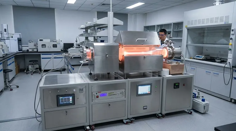
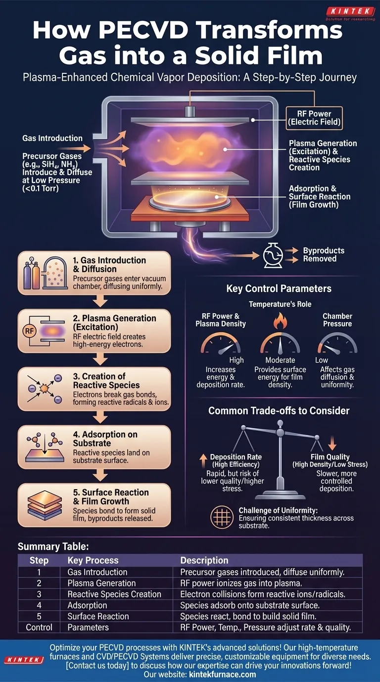
In Plasma-Enhanced Chemical Vapor Deposition (PECVD), a reaction gas transforms into a solid film through a multi-stage process driven by plasma energy. Instead of relying solely on high heat, an electrical field energizes the gas into a plasma state, breaking stable gas molecules into highly reactive fragments. These fragments then travel to the substrate surface, where they chemically react and bond to form a solid, thin film.
The core principle of PECVD is using the energy of a plasma—an ionized gas—to initiate chemical reactions at a much lower temperature than required by conventional methods. This allows for the deposition of high-quality films on substrates that cannot withstand high heat.
The Journey from Gas to Solid: A Step-by-Step Breakdown
The transformation from a free-flowing gas to a precisely engineered solid film is not a single event but a sequence of carefully controlled physical and chemical steps.
Step 1: Gas Introduction and Diffusion
The process begins by introducing specific precursor gases, such as Silane (SiH₄) and Ammonia (NH₃), into a vacuum chamber. These gases are the source materials for the final film.
The chamber is held at a very low pressure (typically below 0.1 Torr) to allow the gas molecules to diffuse freely and uniformly toward the substrate, which is often a silicon wafer.
Step 2: Plasma Generation (The "Excitation")
An electric field, typically generated by a radio-frequency (RF) power supply, is applied across electrodes within the chamber.
This strong electric field accelerates free electrons in the chamber, giving them high kinetic energy.
Step 3: Creation of Reactive Species
These high-energy electrons collide with the neutral, stable precursor gas molecules. The impact is energetic enough to break the chemical bonds of the gas molecules.
This decomposition creates a mix of electrons, ions, and highly reactive species (also known as radicals or reactive groups). This energized, ionized gas mixture is the plasma.
Step 4: Adsorption on the Substrate
The newly created reactive species are chemically unstable and readily seek to form new, more stable bonds.
They diffuse through the plasma and land on the surface of the temperature-controlled substrate, a process called adsorption.
Step 5: Surface Reaction and Film Growth
Once on the surface, the adsorbed species migrate, interact, and undergo chemical reactions with each other. During this stage, they bond to the substrate and to each other, building the solid film layer by layer.
Volatile byproducts of these surface reactions are released and pumped out of the chamber, leaving behind only the desired solid film.
Understanding the Key Control Parameters
The final properties of the film—such as its thickness, density, stress, and refractive index—are not accidental. They are the direct result of precise control over the process conditions.
The Levers of Control
Engineers use several key parameters as levers to tune the film's characteristics. These include the RF power, chamber pressure, gas flow rates, gas mixture composition, and substrate temperature.
RF Power and Plasma Density
Increasing the RF power increases the density and energy of the plasma. This typically accelerates the decomposition of precursor gases and increases the deposition rate. However, excessive power can also lead to film damage or high internal stress.
Temperature's Role
While PECVD is a "low-temperature" process, the substrate temperature is still a critical parameter. It provides the necessary surface energy for adsorbed species to migrate and react properly, directly influencing the final film's density and chemical structure.
Common Trade-offs to Consider
Achieving the perfect film requires balancing competing factors. Understanding these trade-offs is crucial for process optimization.
Deposition Rate vs. Film Quality
A higher deposition rate is often desired for manufacturing efficiency, but it can come at a cost. Rapidly deposited films may have lower density, higher impurity content, or unfavorable stress levels.
Achieving high-quality films often requires a slower, more controlled deposition, allowing atoms sufficient time to settle into an optimal, low-energy state.
The Challenge of Uniformity
Ensuring the film has the same thickness and properties across the entire substrate is a significant engineering challenge. Non-uniform plasma density or temperature gradients across the substrate can lead to variations in the final film.
Optimizing PECVD for Your Goal
The ideal process parameters are entirely dependent on your desired outcome.
- If your primary focus is high deposition speed: You will likely need to increase RF power and precursor gas flow, but remain mindful of the potential negative impacts on film stress and quality.
- If your primary focus is superior film quality (e.g., low stress, high density): Your strategy will involve carefully optimizing a moderate substrate temperature, managing plasma energy, and potentially accepting a slower deposition rate.
- If your primary focus is process repeatability: You must implement rigorous control over all input parameters—gas flow, pressure, temperature, and RF power—to ensure consistent results from one run to the next.
Ultimately, PECVD empowers engineers to create critical materials by using plasma to master chemical reactions at the atomic scale.
Summary Table:
| Step | Key Process | Description |
|---|---|---|
| 1 | Gas Introduction | Precursor gases like SiH₄ and NH₃ are introduced into a vacuum chamber for uniform diffusion. |
| 2 | Plasma Generation | RF power creates an electric field, ionizing the gas into plasma with high-energy electrons. |
| 3 | Reactive Species Creation | Electron collisions break gas bonds, forming reactive ions and radicals for deposition. |
| 4 | Adsorption | Reactive species adsorb onto the substrate surface, initiating film formation. |
| 5 | Surface Reaction | Species react and bond on the surface, building the solid film layer by layer. |
| Control Parameters | RF Power, Temperature, Pressure | Adjust to influence deposition rate, film quality, and uniformity for optimal results. |
Optimize your PECVD processes with KINTEK's advanced solutions! Our high-temperature furnaces, including CVD/PECVD Systems, are engineered with exceptional R&D and in-house manufacturing to deliver precise, customizable equipment for diverse laboratory needs. Whether you're aiming for high deposition rates, superior film quality, or repeatable results, we provide tailored support to enhance your thin film applications. Contact us today to discuss how our expertise can drive your innovations forward!
Visual Guide
Related Products
- Slide PECVD Tube Furnace with Liquid Gasifier PECVD Machine
- RF PECVD System Radio Frequency Plasma Enhanced Chemical Vapor Deposition
- Inclined Rotary Plasma Enhanced Chemical Deposition PECVD Tube Furnace Machine
- Inclined Rotary Plasma Enhanced Chemical Deposition PECVD Tube Furnace Machine
- Multi Heating Zones CVD Tube Furnace Machine for Chemical Vapor Deposition Equipment
People Also Ask
- In which industries is the tube furnace commonly used? Essential for Materials Science, Energy, and More
- What is plasma in the context of PECVD? Unlock Low-Temperature Thin Film Deposition
- What are the typical conditions for plasma-enhanced CVD processes? Achieve Low-Temperature Thin Film Deposition
- What are the main advantages of PECVD tube furnaces compared to CVD tube furnaces? Lower Temp, Faster Deposition, and More
- What role does a Tube Furnace play in the CVD growth of carbon nanotubes? Achieve High-Purity CNT Synthesis


