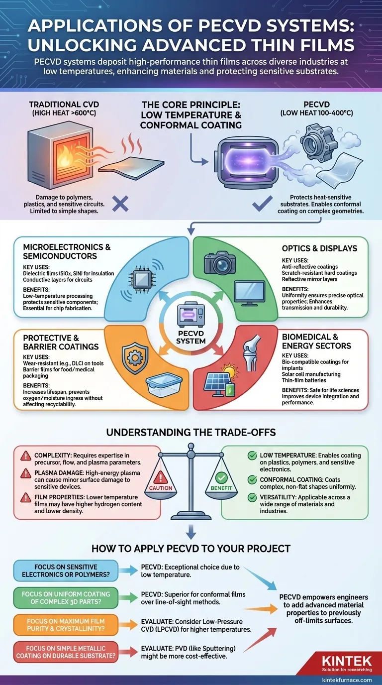
In short, PECVD systems are used across a vast range of industries to deposit high-performance thin films. Key applications are found in microelectronics for creating insulating and conductive layers, in optics for anti-reflective and scratch-resistant coatings, and in packaging to create protective barrier films. The technology's versatility also extends to biomedical devices, solar cells, and wear-resistant coatings for mechanical parts.
The true value of PECVD lies not just in the films it creates, but in its ability to do so at low temperatures. This single advantage opens the door to enhancing materials—from plastic packaging to sensitive electronics—that would be destroyed by traditional high-temperature deposition methods.
The Core Principle: Why Low Temperature Changes Everything
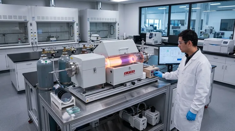
The defining characteristic of Plasma-Enhanced Chemical Vapor Deposition (PECVD) is its use of an energy-rich plasma to initiate chemical reactions, rather than relying solely on high heat. This fundamental difference is what makes it so widely applicable.
Protecting Heat-Sensitive Substrates
Traditional Chemical Vapor Deposition (CVD) often requires temperatures of 600-800°C or higher. Many materials, such as polymers, plastics, and certain integrated circuits, cannot withstand this heat.
PECVD operates at much lower temperatures, typically 100-400°C. This allows for the deposition of high-quality films onto temperature-sensitive substrates without causing damage, warping, or degradation.
Enabling Conformal Coating on Complex Shapes
Unlike many line-of-sight deposition techniques (like evaporation or sputtering), the gas-phase precursors in a PECVD process can flow around and coat complex, three-dimensional objects.
This ability to create a uniform, conformal coating on intricate geometries makes it invaluable for components with non-flat surfaces, from mechanical parts to medical implants.
Key Application Breakdowns
The combination of low temperature, high film quality, and versatility unlocks a diverse set of industrial uses.
In Microelectronics and Semiconductors
This is a primary application for PECVD. It is used to deposit dielectric (insulating) films, such as silicon dioxide (SiO2) and silicon nitride (SiN), which are fundamental for building modern integrated circuits.
These films isolate conductive layers from each other, protect the chip from the environment, and form essential parts of transistors. PECVD is also used for photosensitive and conductive coatings within the microfabrication process.
In Optics and Displays
PECVD is used to apply precise thin films to lenses, mirrors, and display panels. These coatings can be engineered to have specific refractive indices to create anti-reflective properties, enhancing light transmission.
Other optical applications include creating durable, scratch-resistant hard coatings or highly reflective layers for mirrors and other optical components. The process's uniformity is critical for achieving consistent optical performance.
In Protective and Barrier Coatings
For mechanical engineering, PECVD can deposit extremely hard, wear-resistant coatings (like diamond-like carbon) onto tools and components, dramatically increasing their lifespan.
In the food and medical packaging industry, PECVD is used to apply a thin, transparent barrier layer (often silicon-based) to plastic films. This barrier prevents oxygen and moisture from entering, preserving the contents without affecting recyclability.
In Biomedical and Energy Sectors
The low-temperature nature of PECVD is critical for life sciences. It's used to coat medical implants with bio-compatible materials that improve integration with the body and prevent rejection. Other uses include surfaces for cell cultures and advanced drug delivery systems.
In the energy sector, PECVD is a key process for manufacturing photovoltaic cells (solar panels) and developing thin-film materials for next-generation batteries and energy storage.
Understanding the Trade-offs
While powerful, PECVD is not a universal solution. Understanding its operational context is key to successful implementation.
Precursor and Plasma Complexity
The quality of the final film is highly dependent on the precursor gases used, gas flow rates, pressure, and plasma power. Optimizing this multi-variable process requires significant expertise to achieve the desired film properties.
Potential for Plasma-Induced Damage
While the low temperature protects the substrate from thermal damage, the high-energy plasma itself can sometimes cause minor surface damage or introduce impurities if not carefully controlled. This is a critical consideration for extremely sensitive electronic devices.
Film Purity and Density
Because PECVD operates at lower temperatures, the resulting films can sometimes incorporate more hydrogen and have a slightly lower density compared to films grown with high-temperature methods. For applications requiring the absolute highest purity or crystal quality, other methods may be more suitable.
How to Apply This to Your Project
Your choice of deposition technology should be driven entirely by your substrate material and the desired film properties.
- If your primary focus is sensitive electronics or polymer substrates: PECVD is an exceptional choice due to its low-temperature processing, which prevents substrate damage.
- If your primary focus is coating complex 3D parts uniformly: PECVD's ability to create conformal films makes it far superior to line-of-sight deposition techniques.
- If your primary focus is maximum film purity and crystallinity: You should evaluate if PECVD meets your needs or if a higher-temperature method, like Low-Pressure CVD (LPCVD), is necessary.
- If your primary focus is a simple metallic coating on a durable substrate: A simpler physical vapor deposition (PVD) method like sputtering might be more cost-effective.
Ultimately, PECVD empowers engineers to add advanced material properties to surfaces that were previously off-limits to high-temperature enhancement.
Summary Table:
| Application Area | Key Uses | Key Benefits |
|---|---|---|
| Microelectronics & Semiconductors | Dielectric films (e.g., SiO2, SiN), conductive layers | Low-temperature processing, protects sensitive circuits |
| Optics & Displays | Anti-reflective coatings, scratch-resistant layers | Uniform coating, precise optical properties |
| Protective & Barrier Coatings | Wear-resistant coatings (e.g., DLC), barrier films for packaging | Conformal coating on complex shapes, enhances durability |
| Biomedical & Energy | Bio-compatible coatings for implants, solar cell manufacturing | Enables use on heat-sensitive substrates, improves device performance |
Unlock the full potential of PECVD for your projects with KINTEK! Leveraging exceptional R&D and in-house manufacturing, we provide advanced high-temperature furnace solutions tailored to your needs. Our product line, including Muffle, Tube, Rotary Furnaces, Vacuum & Atmosphere Furnaces, and CVD/PECVD Systems, is complemented by strong deep customization capabilities to precisely meet unique experimental requirements. Whether you're in microelectronics, optics, or biomedical sectors, our expertise ensures optimal performance and efficiency. Contact us today to discuss how we can enhance your laboratory's capabilities and drive innovation!
Visual Guide
Related Products
- RF PECVD System Radio Frequency Plasma Enhanced Chemical Vapor Deposition
- Slide PECVD Tube Furnace with Liquid Gasifier PECVD Machine
- Inclined Rotary Plasma Enhanced Chemical Deposition PECVD Tube Furnace Machine
- Inclined Rotary Plasma Enhanced Chemical Deposition PECVD Tube Furnace Machine
- Cylindrical Resonator MPCVD Machine System for Lab Diamond Growth
People Also Ask
- What are some promising applications of PECVD-prepared 2D materials? Unlock Advanced Sensing and Optoelectronics
- What are the system specifications of the PECVD system? Unlock Precision Thin-Film Deposition
- How are deposition rates and film properties controlled in PECVD? Master Key Parameters for Optimal Thin Films
- What are the limitations of PECVD? Overcome Process Control and Cost Challenges
- What is RF in PECVD? A Critical Control for Plasma Deposition


