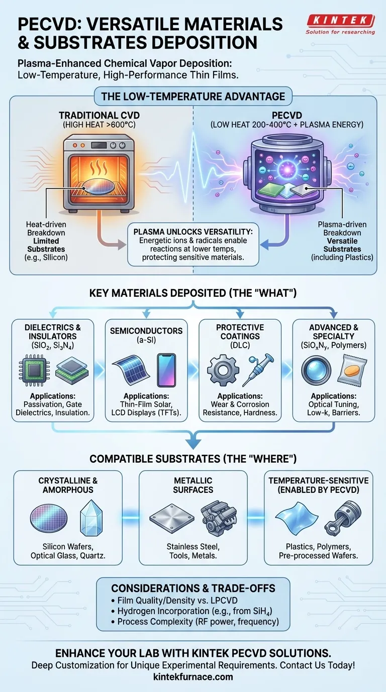
Fundamentally, Plasma-Enhanced Chemical Vapor Deposition (PECVD) is a highly versatile technique capable of depositing a broad array of materials onto many different surfaces. The most common materials include dielectrics like silicon nitride (Si₃N₄) and silicon dioxide (SiO₂), semiconductors like amorphous silicon (a-Si), and protective coatings like Diamond-Like Carbon (DLC). These films can be applied to substrates ranging from silicon wafers and quartz to stainless steel and even plastics.
The core reason for PECVD's versatility is its low-temperature operation. By using an energy-rich plasma rather than high heat to drive chemical reactions, PECVD can deposit high-quality thin films on substrates that would be damaged or destroyed by other high-temperature methods.
Why Plasma Unlocks Material Versatility
Traditional Chemical Vapor Deposition (CVD) requires very high temperatures (often >600°C) to provide the energy needed to break down precursor gases and form a film. PECVD achieves the same outcome at much lower temperatures, typically between 200°C and 400°C.
The Role of Plasma Energy
In a PECVD chamber, an electric field is applied to a low-pressure gas, creating a plasma. This plasma is a highly energetic state of matter containing ions, electrons, and neutral radicals.
These energetic particles bombard the precursor gas molecules, breaking them apart into reactive species. These species then travel to the substrate surface and react to form the desired thin film, without needing extreme heat.
Key Material Categories Deposited by PECVD
PECVD is not a single process but a family of processes tailored for different materials. The choice of precursor gases, plasma power, and temperature determines the final film.
Dielectrics and Insulators (SiO₂, Si₃N₄)
This is the most common application of PECVD, especially in the semiconductor industry. Films like silicon dioxide (SiO₂) and silicon nitride (Si₃N₄) are excellent electrical insulators.
They are used as passivation layers to protect microchips from moisture and contamination, as gate dielectrics in transistors, and as insulating layers between metal wiring on a chip.
Semiconductors (a-Si)
PECVD is the dominant method for depositing amorphous silicon (a-Si). Unlike crystalline silicon, amorphous silicon lacks a long-range ordered structure.
This material is critical for thin-film solar cells and is the active layer in the thin-film transistors (TFTs) that control the pixels in LCD displays for TVs, laptops, and phones.
Protective & Functional Coatings (DLC)
Diamond-Like Carbon (DLC) films are extremely hard, chemically inert, and have a very low coefficient of friction.
Deposited via PECVD, DLC creates a durable, wear-resistant coating on tools, medical implants, automotive engine parts, and optical components to protect them from scratches and corrosion.
Advanced and Specialty Films
The flexibility of PECVD allows for the deposition of more complex or niche materials. This includes silicon oxynitride (SiOxNy) for tuning optical properties, low-k dielectrics to improve microprocessor speed, and even organic polymer films for applications like food packaging barriers or biomedical device coatings.
Compatible Substrates: The Advantage of Low Temperature
The low-temperature nature of PECVD is what opens the door to its wide range of compatible substrates.
Crystalline and Amorphous Substrates
PECVD is routinely used on traditional substrates like silicon wafers, optical glass, and quartz. Because the process is less thermally aggressive, it reduces the risk of wafer warpage or stress.
It also works exceptionally well on metallic substrates like stainless steel, where it is often used to apply DLC or other protective coatings.
Temperature-Sensitive Substrates
This is where PECVD truly excels. Its low operating temperature allows for deposition on materials that cannot withstand traditional CVD. This includes polymers and plastics, enabling applications in flexible electronics, and pre-processed silicon wafers that already have sensitive metallic structures fabricated on them.
Understanding the Trade-offs
While powerful, PECVD is not without its limitations. Objectivity requires acknowledging where other methods may be superior.
Film Quality and Purity
PECVD films are generally of very high quality, but they can have a lower density and higher defect count than films grown at higher temperatures using methods like Low-Pressure CVD (LPCVD).
Hydrogen Incorporation
PECVD precursor gases often contain hydrogen (e.g., Silane - SiH₄). The plasma process can lead to a significant amount of hydrogen being incorporated into the final film, which can sometimes impact the film's electrical or mechanical properties.
Process Complexity
Controlling a plasma adds variables to the deposition process, such as RF power and frequency. This can make process optimization more complex compared to a purely thermal process.
Making the Right Choice for Your Application
Selecting a deposition method depends entirely on your end goal. PECVD is a powerful tool when its specific advantages align with your needs.
- If your primary focus is microelectronic device fabrication: PECVD is the industry standard for depositing high-quality silicon nitride and silicon dioxide passivation and inter-metal dielectric layers at temperatures that won't damage existing circuitry.
- If your primary focus is creating hard, wear-resistant surfaces: Explore Diamond-Like Carbon (DLC) films deposited via PECVD, especially for coating metallic, glass, or even polymer substrates.
- If your primary focus is thin-film solar cells or displays: PECVD is the essential technique for depositing the amorphous silicon active layers required for these large-area electronic devices.
- If your primary focus is coating temperature-sensitive materials: PECVD is one of the few methods capable of depositing high-quality inorganic films onto plastics, polymers, or other low-melting-point substrates.
By understanding these principles, you can effectively leverage PECVD to create advanced materials tailored to your specific engineering goal.
Summary Table:
| Category | Materials | Substrates | Key Applications |
|---|---|---|---|
| Dielectrics | Silicon Nitride (Si₃N₄), Silicon Dioxide (SiO₂) | Silicon wafers, Quartz | Passivation, Insulation in microelectronics |
| Semiconductors | Amorphous Silicon (a-Si) | Glass, Silicon wafers | Thin-film solar cells, LCD displays |
| Protective Coatings | Diamond-Like Carbon (DLC) | Stainless steel, Plastics | Wear resistance, Corrosion protection |
| Advanced Films | Silicon Oxynitride (SiOxNy), Low-k dielectrics | Various, including polymers | Optical tuning, Microprocessor speed enhancement |
Ready to enhance your lab's capabilities with advanced PECVD solutions? KINTEK leverages exceptional R&D and in-house manufacturing to provide diverse laboratories with high-temperature furnace systems, including CVD/PECVD Systems. Our strong deep customization capability ensures we precisely meet your unique experimental requirements for depositing materials on various substrates. Contact us today to discuss how our tailored solutions can drive your research forward!
Visual Guide
Related Products
- Slide PECVD Tube Furnace with Liquid Gasifier PECVD Machine
- RF PECVD System Radio Frequency Plasma Enhanced Chemical Vapor Deposition
- Inclined Rotary Plasma Enhanced Chemical Deposition PECVD Tube Furnace Machine
- Inclined Rotary Plasma Enhanced Chemical Deposition PECVD Tube Furnace Machine
- Multi Heating Zones CVD Tube Furnace Machine for Chemical Vapor Deposition Equipment
People Also Ask
- What are the main advantages of PECVD tube furnaces compared to CVD tube furnaces? Lower Temp, Faster Deposition, and More
- What are the advantages of using a tube furnace CVD system for Cu(111)/graphene? Superior Scalability and Quality
- How does PECVD equipment contribute to TOPCon bottom cells? Mastering Hydrogenation for Maximum Solar Efficiency
- What are the typical conditions for plasma-enhanced CVD processes? Achieve Low-Temperature Thin Film Deposition
- How does a hydrogen reduction environment in an industrial tube furnace facilitate gold-copper alloy microspheres?


