In modern device fabrication, the significance of Plasma-Enhanced Chemical Vapor Deposition (PECVD) lies in its unique ability to deposit high-quality thin films at low temperatures. This capability is not merely an improvement but a fundamental enabler for manufacturing advanced microelectronics, biomedical devices, and optical components where high-temperature processes would cause catastrophic damage.
PECVD's true value is its role as a problem-solver. By decoupling the deposition process from high heat, it unlocks the ability to build sophisticated devices on thermally sensitive substrates, which would otherwise be impossible.
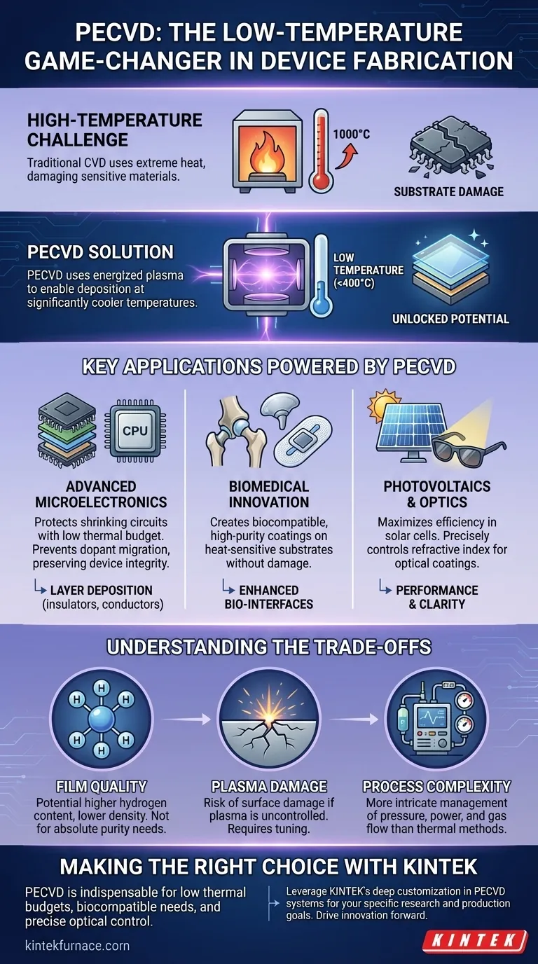
Why Low Temperature is a Game-Changer
Traditional deposition methods, like furnace-driven Chemical Vapor Deposition (CVD), often require extremely high temperatures. While effective, this heat imposes severe limitations. PECVD overcomes this by using an energized plasma to drive the chemical reactions needed for film deposition, allowing the process to run hundreds of degrees cooler.
Protecting Advanced Microelectronics
As circuits shrink, the "thermal budget"—the total amount of heat a device can tolerate during manufacturing—decreases dramatically.
High temperatures can cause dopants (impurities intentionally added to silicon) to migrate from their intended locations. This migration can short-circuit transistors or alter their electrical properties, destroying the device.
PECVD deposits essential insulating and conductive layers well below these critical temperature thresholds, preserving the integrity of the intricate, multi-layered circuitry.
Enabling Biomedical Innovation
The fabrication of medical implants and biosensors requires depositing materials onto substrates that are often incompatible with high heat.
PECVD excels at creating biocompatible, high-purity coatings on medical implants. These films enhance performance and longevity without damaging the underlying device or using temperatures that would compromise sensitive biological materials.
For biosensors, the process deposits the uniform, high-quality films needed for reliable performance while protecting the delicate sensor components.
Advancing Photovoltaics and Optics
PECVD is a cornerstone of manufacturing for thin-film solar cells and a wide array of optical devices.
In photovoltaics, it is used to deposit layers like amorphous silicon and silicon nitride. The ability to control film properties at low temperatures is crucial for maximizing the efficiency and performance of solar panels.
For optical coatings on items like sunglasses or data storage systems, PECVD allows for precise control over the film's refractive index, creating effective anti-reflection and glare-reduction surfaces.
Understanding the Trade-offs
While powerful, PECVD is not a universal solution. Understanding its limitations is key to using it effectively. The use of plasma introduces complexities and trade-offs compared to purely thermal processes.
Film Quality vs. Temperature
Films deposited via PECVD can sometimes have a higher concentration of hydrogen and a lower density than films grown at very high temperatures. For applications demanding the absolute highest film purity or dielectric strength, a higher-temperature process might still be necessary if the substrate can tolerate it.
Potential for Plasma Damage
The same energized plasma that enables low-temperature deposition can, if not properly controlled, cause physical or electrical damage to the substrate surface. Process engineers must carefully tune plasma parameters to deposit the film effectively without harming the underlying device layers.
Process Complexity
Managing a stable, uniform plasma adds a layer of complexity to the deposition process. It requires sophisticated equipment and precise control over variables like pressure, power, and gas flow rates, making it a more intricate process than simple thermal deposition.
Making the Right Choice for Your Application
PECVD's low-temperature capability is its defining feature, making it indispensable across multiple high-tech fields. The decision to use it depends entirely on your specific manufacturing constraints and performance goals.
- If your primary focus is advanced microelectronics: PECVD is critical for working within shrinking thermal budgets and preventing dopant migration.
- If your primary focus is biomedical devices: PECVD is the premier choice for applying high-purity, biocompatible coatings onto thermally sensitive materials.
- If your primary focus is photovoltaics or optics: PECVD offers the precise control over film composition and refractive index needed to maximize device efficiency and performance.
Ultimately, PECVD empowers engineers to build the next generation of technology by removing the restrictive barrier of high-temperature processing.
Summary Table:
| Aspect | Key Insights |
|---|---|
| Low-Temperature Capability | Enables deposition on thermally sensitive substrates, preventing damage in microelectronics and biomedical devices. |
| Applications | Critical for advanced microelectronics (prevents dopant migration), biomedical coatings (biocompatible films), and photovoltaics/optics (controls refractive index). |
| Trade-offs | Films may have higher hydrogen content; plasma can cause damage if uncontrolled; process is more complex than thermal methods. |
| Decision Factors | Choose PECVD for low thermal budgets, biocompatible needs, or precise optical control; consider alternatives for highest purity if substrates tolerate heat. |
Unlock the Power of PECVD for Your Lab
At KINTEK, we specialize in advanced high-temperature furnace solutions, including CVD/PECVD systems, tailored to meet the unique demands of modern device fabrication. Leveraging our exceptional R&D and in-house manufacturing, we offer deep customization to ensure precise control for applications in microelectronics, biomedical devices, and optics. Whether you need to overcome thermal limitations or enhance film quality, our expertise can drive your innovations forward.
Contact us today to discuss how our PECVD systems and other furnace solutions can elevate your research and production efficiency!
Visual Guide
Related Products
- Slide PECVD Tube Furnace with Liquid Gasifier PECVD Machine
- RF PECVD System Radio Frequency Plasma Enhanced Chemical Vapor Deposition
- Inclined Rotary Plasma Enhanced Chemical Deposition PECVD Tube Furnace Machine
- Inclined Rotary Plasma Enhanced Chemical Deposition PECVD Tube Furnace Machine
- Multi Heating Zones CVD Tube Furnace Machine for Chemical Vapor Deposition Equipment
People Also Ask
- What is plasma in the context of PECVD? Unlock Low-Temperature Thin Film Deposition
- What role does a Tube Furnace play in the CVD growth of carbon nanotubes? Achieve High-Purity CNT Synthesis
- What are the typical conditions for plasma-enhanced CVD processes? Achieve Low-Temperature Thin Film Deposition
- What are the disadvantages of tube furnace cracking when processing heavy raw materials? Avoid Costly Downtime and Inefficiency
- What are the advantages of using a tube furnace CVD system for Cu(111)/graphene? Superior Scalability and Quality


