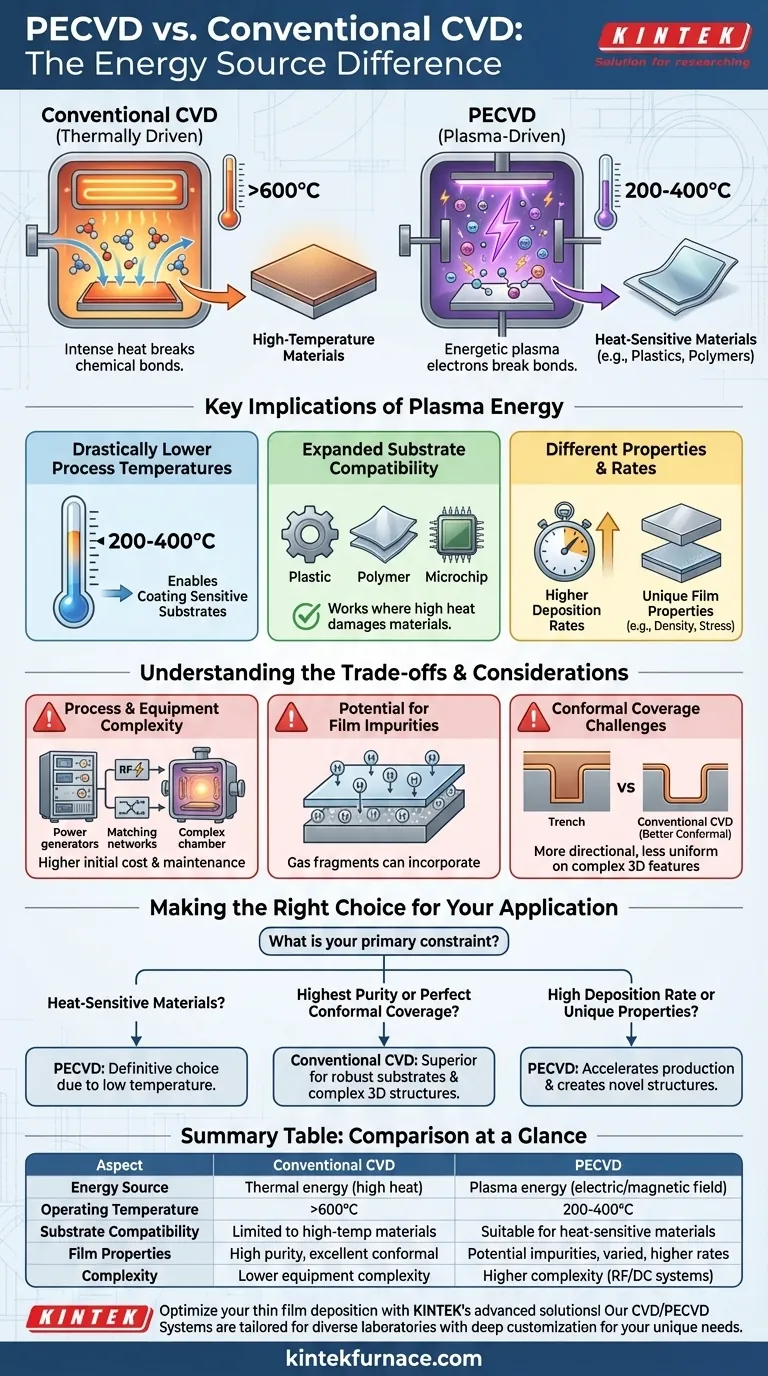
At its core, Plasma Enhanced Chemical Vapor Deposition (PECVD) is a process for depositing thin films that substitutes the intense heat of conventional CVD with the energy from a plasma. This fundamental difference allows PECVD to operate at much lower temperatures, making it a critical technology for coating materials that cannot withstand high heat.
The essential choice between PECVD and conventional CVD is a trade-off between thermal energy and plasma energy. PECVD's use of plasma enables high-quality film deposition at significantly lower temperatures, expanding its use to heat-sensitive materials where conventional CVD is not viable.
The Fundamental Difference: Energy Source
The distinction between these two powerful techniques lies entirely in how they supply the energy needed to drive the chemical reaction.
Conventional CVD: A Thermally Driven Process
Conventional Chemical Vapor Deposition (CVD) relies purely on thermal energy. The substrate is heated to very high temperatures, which energizes the precursor gases flowing over it.
This intense heat provides the activation energy required to break the chemical bonds of the precursor molecules, allowing them to react and deposit a solid film onto the hot substrate surface.
PECVD: A Plasma-Driven Process
PECVD introduces a second energy source: plasma. An electric or magnetic field is applied to the precursor gas inside the reaction chamber, igniting it into a plasma.
This plasma is a partially ionized gas containing highly energetic electrons. These electrons, not the substrate's heat, collide with and break apart the precursor gas molecules, creating reactive ions and radicals that are then deposited onto the much cooler substrate.
Key Implications of Using Plasma
Substituting thermal energy with plasma energy creates several critical advantages that dictate when and why PECVD is used.
Drastically Lower Process Temperatures
This is the most significant benefit of PECVD. While conventional CVD often requires temperatures well above 600°C, PECVD typically operates in the 200-400°C range.
This reduction is possible because the plasma, not heat, is doing the heavy lifting of breaking down the stable precursor gases.
Expanded Substrate Compatibility
The low operating temperature directly enables the coating of temperature-sensitive materials.
Substrates like plastics, polymers, and certain semiconductor devices would be damaged, melted, or destroyed by the high heat of conventional CVD. PECVD makes it possible to deposit high-performance films on these materials.
Different Film Properties and Deposition Rates
The unique chemical environment of the plasma can create different reactive species than a purely thermal process.
This can lead to films with distinct properties, such as improved density or reduced stress. In many cases, the high reactivity within the plasma also allows for higher deposition rates than conventional CVD.
Understanding the Trade-offs
While powerful, PECVD is not a universal replacement for conventional CVD. The choice involves clear trade-offs tied to the underlying physics.
Process and Equipment Complexity
A PECVD system is inherently more complex. It requires RF or DC power generators, impedance matching networks, and robust chamber designs to generate and contain the plasma. This can translate to higher initial equipment cost and maintenance.
Potential for Film Impurities
Because the plasma breaks down precursors so aggressively, fragments of the gas molecules (like hydrogen) can become incorporated into the growing film. This can affect the film's optical, electrical, or mechanical properties, which may be undesirable for certain high-purity applications.
Conformal Coverage Challenges
Conventional CVD, particularly Low-Pressure CVD (LPCVD), often excels at creating highly conformal films that uniformly coat complex 3D structures. The PECVD process can be more directional, sometimes leading to thinner coatings on the sidewalls of features compared to the top surfaces.
Making the Right Choice for Your Application
Selecting the correct deposition method requires matching the process capabilities to your project's primary constraint.
- If your primary focus is coating heat-sensitive materials: PECVD is the definitive and often only choice due to its low operating temperature.
- If your primary focus is the highest possible film purity or perfect conformal coverage on a robust substrate: Conventional thermal CVD (like LPCVD or APCVD) may be the superior option.
- If your primary focus is a high deposition rate or achieving unique film properties: PECVD provides a pathway to accelerate production and create novel material structures not possible with thermal methods alone.
Ultimately, understanding the energy source—thermal versus plasma—is the key to selecting the right deposition technology for your specific material and performance goals.
Summary Table:
| Aspect | Conventional CVD | PECVD |
|---|---|---|
| Energy Source | Thermal energy (high heat) | Plasma energy (electric/magnetic field) |
| Operating Temperature | Typically >600°C | Typically 200-400°C |
| Substrate Compatibility | Limited to high-temperature materials | Suitable for heat-sensitive materials (e.g., plastics, polymers) |
| Film Properties | High purity, excellent conformal coverage | Potential for impurities, varied properties, higher deposition rates |
| Complexity | Lower equipment complexity | Higher complexity with RF/DC power systems |
Optimize your thin film deposition with KINTEK's advanced solutions! Leveraging exceptional R&D and in-house manufacturing, we provide high-temperature furnace systems like CVD/PECVD Systems tailored for diverse laboratories. Our strong deep customization capability ensures precise alignment with your unique experimental needs, whether for heat-sensitive materials or high-purity applications. Contact us today to discuss how our expertise can enhance your research and production efficiency!
Visual Guide
Related Products
- RF PECVD System Radio Frequency Plasma Enhanced Chemical Vapor Deposition
- Slide PECVD Tube Furnace with Liquid Gasifier PECVD Machine
- Inclined Rotary Plasma Enhanced Chemical Deposition PECVD Tube Furnace Machine
- Inclined Rotary Plasma Enhanced Chemical Deposition PECVD Tube Furnace Machine
- Cylindrical Resonator MPCVD Machine System for Lab Diamond Growth
People Also Ask
- How are deposition rates and film properties controlled in PECVD? Master Key Parameters for Optimal Thin Films
- What are some promising applications of PECVD-prepared 2D materials? Unlock Advanced Sensing and Optoelectronics
- What is the role of RF power in PECVD and how does the RF-PECVD process work? Master Thin Film Deposition Control
- What are the key advantages of PECVD technology? Achieve Low-Temperature, High-Quality Thin Film Deposition
- How does film quality compare between PECVD and CVD? Choose the Best Method for Your Substrate


