In short, Plasma-Enhanced Chemical Vapor Deposition (PECVD) is a foundational manufacturing process used to deposit high-performance thin films onto various materials. Its applications are widespread, serving as a critical step in producing semiconductors, solar cells, LEDs, optical components, and protective coatings for medical and electronic devices.
The central value of PECVD is its ability to create high-quality, durable films at significantly lower temperatures than traditional methods. This use of plasma is what makes it indispensable for manufacturing modern electronics and other sensitive, high-performance components that would be damaged by excessive heat.
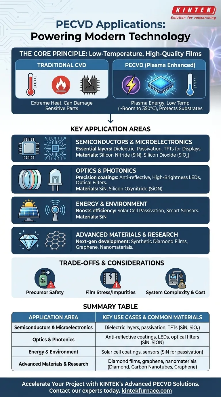
Why PECVD is a Go-To Technology
The Core Principle: A Low-Temperature Solution
Traditional Chemical Vapor Deposition (CVD) requires very high temperatures to trigger the chemical reactions that form a film. This intense heat can easily damage or destroy sensitive components, such as integrated circuits or polymers.
PECVD solves this problem by using an electric field to generate plasma, an energized state of gas. This plasma provides the energy needed for the chemical reactions, allowing for deposition to occur at much lower temperatures—often from room temperature to around 350°C.
The Result: High-Quality, Functional Films
This controlled, low-temperature process produces films that are dense, uniform, and adhere strongly to the substrate. These films are engineered to serve specific functions, such as electrical insulation, corrosion resistance, or modifying optical properties.
Key Application Areas in Detail
Semiconductor and Microelectronics Fabrication
This is the most common and critical application of PECVD. It is used to create essential layers within microchips and other electronic devices.
Key films include dielectric layers for insulating conductive paths, passivation layers for protecting the chip surface from contamination and moisture, and functional layers in Thin-Film Transistors (TFTs) used in modern displays. Silicon nitride (SiN) is a particularly common film for these purposes.
Optics and Photonics
PECVD provides the precise control needed to build complex optical structures layer by layer. This enables the manufacturing of high-performance components for communications and displays.
Applications include creating anti-reflective coatings on lenses, fabricating high-brightness LEDs, and producing specialized filters for optical fiber communications and display technologies.
Energy and Environmental Technology
The technology is vital for renewable energy and smart infrastructure. In solar cell manufacturing, PECVD is used to deposit anti-reflective and passivation layers that significantly increase the efficiency of converting sunlight into electricity.
It is also used to create the sensitive films in sensors for HVAC systems, smart city utility meters, and biosensors.
Advanced Materials and Research
PECVD is a versatile tool for developing next-generation materials. Specialized systems, such as microwave plasma CVD, are used to grow high-purity synthetic diamond films for use in optics, electronics, and durable tooling.
The process is also employed in the synthesis of graphene, carbon nanotubes, and other nanomaterials with unique electronic and mechanical properties.
Understanding the Trade-offs and Limitations
While powerful, PECVD is not a universal solution. Understanding its limitations is key to using it effectively.
Precursor Chemistry and Safety
The precursor gases used in PECVD can be corrosive, flammable, or toxic. Managing these materials requires significant investment in facility safety protocols, gas handling systems, and abatement.
Film Impurities and Stress
The plasma environment can incorporate elements like hydrogen into the deposited film, which can sometimes affect its electrical or mechanical properties. Additionally, the deposited films can have internal stress, which must be managed to prevent cracking or delamination, especially in thick layers.
System Complexity and Cost
PECVD systems are complex high-vacuum tools that require significant capital investment and expertise to operate and maintain. The cost and complexity make it most suitable for high-value applications where film quality is paramount.
Making the Right Choice for Your Goal
Deciding if PECVD is appropriate depends entirely on your technical and commercial objectives.
- If your primary focus is mass-producing robust electronic devices: PECVD is the industry standard for depositing reliable insulating and protective films without damaging the underlying integrated circuits.
- If your primary focus is advanced optics or displays: Use PECVD for its unmatched precision in depositing multi-layer coatings with specific refractive indices and anti-reflective properties.
- If your primary focus is creating durable protective coatings: PECVD excels at creating dense, pinhole-free barrier layers for medical devices, sensors, and components exposed to harsh environments.
- If your primary focus is research and development of novel materials: PECVD offers a highly controllable platform for experimenting with and synthesizing high-performance materials like diamond, graphene, and custom alloys.
Ultimately, PECVD is an enabling technology that translates material science breakthroughs into the functional, reliable products that power our modern world.
Summary Table:
| Application Area | Key Use Cases | Common Materials Deposited |
|---|---|---|
| Semiconductors & Microelectronics | Dielectric layers, passivation, TFTs | Silicon Nitride (SiN), Silicon Dioxide (SiO₂) |
| Optics & Photonics | Anti-reflective coatings, LEDs, optical filters | Silicon Nitride (SiN), Silicon Oxynitride (SiON) |
| Energy & Environment | Solar cell coatings, sensors | Silicon Nitride (SiN) for passivation |
| Advanced Materials & Research | Diamond films, graphene, nanomaterials | Diamond, Carbon Nanotubes, Graphene |
Ready to integrate PECVD technology into your manufacturing or research?
At KINTEK, we leverage our exceptional R&D and in-house manufacturing to provide advanced PECVD solutions tailored to your specific needs. Whether you are developing next-generation semiconductors, high-efficiency solar cells, or durable optical coatings, our deep customization capabilities ensure your unique experimental and production requirements are met precisely.
Contact our experts today to discuss how our PECVD systems can accelerate your project's success.
Visual Guide
Related Products
- RF PECVD System Radio Frequency Plasma Enhanced Chemical Vapor Deposition
- Slide PECVD Tube Furnace with Liquid Gasifier PECVD Machine
- Inclined Rotary Plasma Enhanced Chemical Deposition PECVD Tube Furnace Machine
- Inclined Rotary Plasma Enhanced Chemical Deposition PECVD Tube Furnace Machine
- MPCVD Machine System Reactor Bell-jar Resonator for Lab and Diamond Growth
People Also Ask
- How are deposition rates and film properties controlled in PECVD? Master Key Parameters for Optimal Thin Films
- How does film quality compare between PECVD and CVD? Choose the Best Method for Your Substrate
- How is silicon dioxide deposited from tetraethylorthosilicate (TEOS) in PECVD? Achieve Low-Temperature, High-Quality SiO2 Films
- What are the key advantages of PECVD technology? Achieve Low-Temperature, High-Quality Thin Film Deposition
- What are some promising applications of PECVD-prepared 2D materials? Unlock Advanced Sensing and Optoelectronics


