The single greatest advantage of PECVD is its ability to deposit high-quality films at significantly lower temperatures than traditional Chemical Vapor Deposition (CVD). By using an energy-rich plasma to drive chemical reactions instead of high heat, PECVD allows for the coating of temperature-sensitive materials like polymers and plastics that would be damaged or destroyed by conventional methods.
PECVD fundamentally decouples the deposition process from thermal energy. This shift allows for rapid, high-quality film growth on a vast range of substrates, unlocking material combinations and performance characteristics that are impossible to achieve with high-temperature techniques.
The Core Advantage: Overcoming Thermal Limitations
The primary reason to choose PECVD is its ability to bypass the need for extreme heat, which has several critical downstream benefits.
Drastically Lower Deposition Temperatures
Traditional CVD requires very high temperatures, often in the range of 400–2000 °C, to provide the necessary activation energy for chemical reactions to occur.
PECVD replaces this thermal energy with energy from a plasma. This allows the process to run at much lower temperatures, from 350 °C down to room temperature, enabling deposition on delicate substrates.
Reduced Thermal Stress and Cracking
When a film and a substrate with different thermal expansion coefficients are heated and cooled, stress builds up at their interface. This can lead to poor adhesion or cracking.
By operating at lower temperatures, PECVD minimizes this thermal stress, resulting in better film adhesion and a much lower likelihood of cracking, which enhances the overall durability and electrical performance of the device.
Superior Film Quality and Control
Beyond temperature, PECVD provides a level of process control that directly translates to higher-quality and more consistent films.
High-Quality Film Formation
The unique deposition mechanism of PECVD results in dense, high-quality films. This process yields coatings with fewer pinholes and excellent uniformity across the entire substrate surface.
Excellent Uniformity and Conformity
PECVD is known for its ability to create films of highly uniform thickness, even over complex, non-flat topographies. This is often referred to as good "step coverage," ensuring that intricate device structures are coated evenly.
Precise Control Over Film Properties
The characteristics of the plasma can be finely tuned by adjusting parameters like gas composition, pressure, and RF power frequency. This allows for precise control over the final film's properties, such as its stoichiometry, density, and internal stress.
Efficiency and Versatility in Production
For manufacturing environments, PECVD offers significant advantages in speed and flexibility.
Significantly Higher Deposition Rates
The plasma-enhanced reactions proceed much more quickly than their thermally-driven counterparts. For some materials, such as silicon nitride, deposition rates can be over 100 times faster than with conventional CVD, drastically increasing manufacturing throughput.
Wide Range of Materials
PECVD is an extremely versatile technique. It can be used to deposit a broad spectrum of materials, including insulators (dielectrics like silicon dioxide), semiconductors (like amorphous silicon), and even some conductive layers.
Enhanced Chemical and Physical Properties
The resulting films often exhibit excellent practical characteristics. These include strong adhesion to the substrate, high resistance to solvents and corrosion, and excellent chemical and thermal stability.
Understanding the Trade-offs
While powerful, PECVD is not a universal solution. Its advantages come with considerations that must be weighed for any given application.
Film Composition Complexity
The plasma environment is highly reactive and can lead to the incorporation of other elements, such as hydrogen, from precursor gases into the film. While this can sometimes be controlled or even beneficial, it can also unintentionally alter the film's desired electrical or optical properties.
Equipment and Process Complexity
A PECVD system, with its vacuum chamber, gas handling, and RF plasma generation hardware, is inherently more complex and expensive than simpler atmospheric deposition methods. Achieving optimal results requires careful control over multiple process parameters.
Potential for Plasma-Induced Damage
The high-energy ions within the plasma can, in some cases, cause physical damage to the substrate surface. For extremely sensitive materials, this bombardment can be a limiting factor that requires careful process tuning to mitigate.
Making the Right Choice for Your Application
Selecting the right deposition technique requires aligning its capabilities with your primary goal.
- If your primary focus is coating heat-sensitive materials: PECVD is the definitive choice due to its low-temperature operation, which protects substrates like plastics and polymers.
- If your primary focus is high-throughput manufacturing: PECVD's rapid deposition rates offer a clear and significant advantage over slower, traditional CVD methods.
- If your primary focus is creating precisely engineered thin films: The granular control over plasma parameters makes PECVD ideal for tuning film stress, stoichiometry, and density.
- If your primary focus is coating robust substrates with minimal cost: Simpler, non-plasma thermal CVD or physical vapor deposition methods may be more economical if the advanced capabilities of PECVD are not required.
Ultimately, PECVD empowers engineers and scientists to build better devices by removing the restrictive barrier of high temperature.
Summary Table:
| Advantage | Key Benefit |
|---|---|
| Low-Temperature Operation | Enables coating of heat-sensitive materials (e.g., polymers) |
| Superior Film Quality | Dense, uniform films with excellent conformity and fewer pinholes |
| High Deposition Rates | Significantly faster than traditional CVD, boosting throughput |
| Precise Process Control | Tunable film properties (stress, stoichiometry, density) |
| Minimized Thermal Stress | Reduces cracking and improves film adhesion |
Ready to leverage PECVD's advantages for your application?
KINTEK's advanced PECVD systems are engineered to deliver the precise, low-temperature deposition capabilities you need. Whether you are working with delicate polymers, require high-throughput manufacturing, or need to fine-tune specific film properties, our expertise in high-temperature furnace solutions and strong deep customization capabilities ensures we can provide a system tailored to your unique experimental and production requirements.
Contact us today to discuss how our PECVD technology can help you build better devices. Get in touch via our contact form
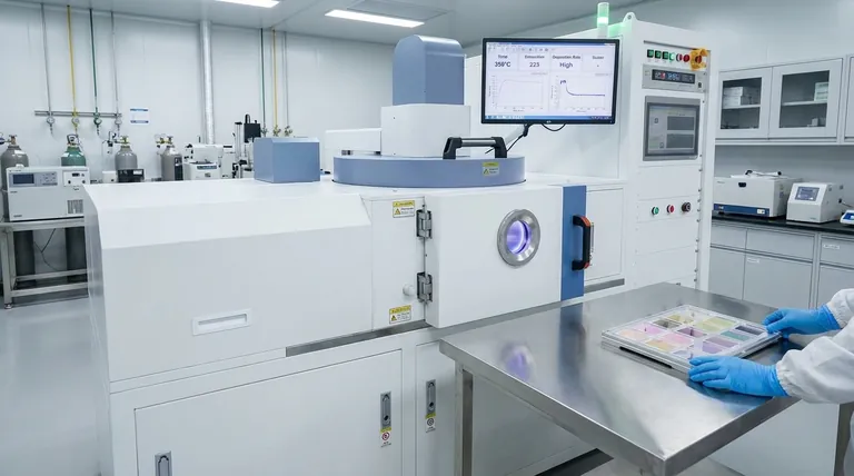
Visual Guide

Related Products
- Slide PECVD Tube Furnace with Liquid Gasifier PECVD Machine
- RF PECVD System Radio Frequency Plasma Enhanced Chemical Vapor Deposition
- Inclined Rotary Plasma Enhanced Chemical Deposition PECVD Tube Furnace Machine
- Inclined Rotary Plasma Enhanced Chemical Deposition PECVD Tube Furnace Machine
- Multi Heating Zones CVD Tube Furnace Machine for Chemical Vapor Deposition Equipment
People Also Ask
- What are the advantages of using a tube furnace CVD system for Cu(111)/graphene? Superior Scalability and Quality
- What are the typical conditions for plasma-enhanced CVD processes? Achieve Low-Temperature Thin Film Deposition
- How does a hydrogen reduction environment in an industrial tube furnace facilitate gold-copper alloy microspheres?
- What plasma source is used in PE-CVD tube furnaces? Unlock Low-Temperature, High-Quality Deposition
- What are the main advantages of PECVD tube furnaces compared to CVD tube furnaces? Lower Temp, Faster Deposition, and More


