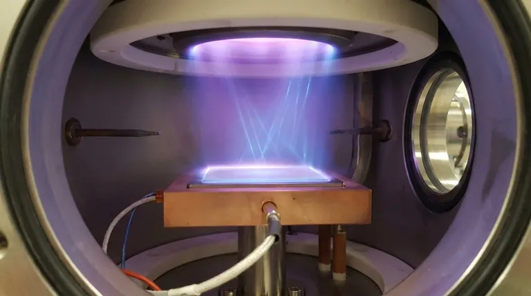
The second key benefit of performing deposition within a plasma discharge is the creation of energetic ion bombardment on the growing film's surface. While the first benefit of Plasma-Enhanced Chemical Vapor Deposition (PECVD) is the ability to deposit films at low temperatures, this second benefit actively improves the material quality of the film itself. This occurs because the plasma's inherent physics create a natural accelerating field that directs ions forcefully onto the substrate.
The crucial insight is that a plasma isn't just a source of energy to drive chemical reactions; it's an active tool for engineering the film's properties. The ion bombardment it generates helps densify the film, enhance its adhesion, and control its internal stress in ways that purely thermal processes cannot.
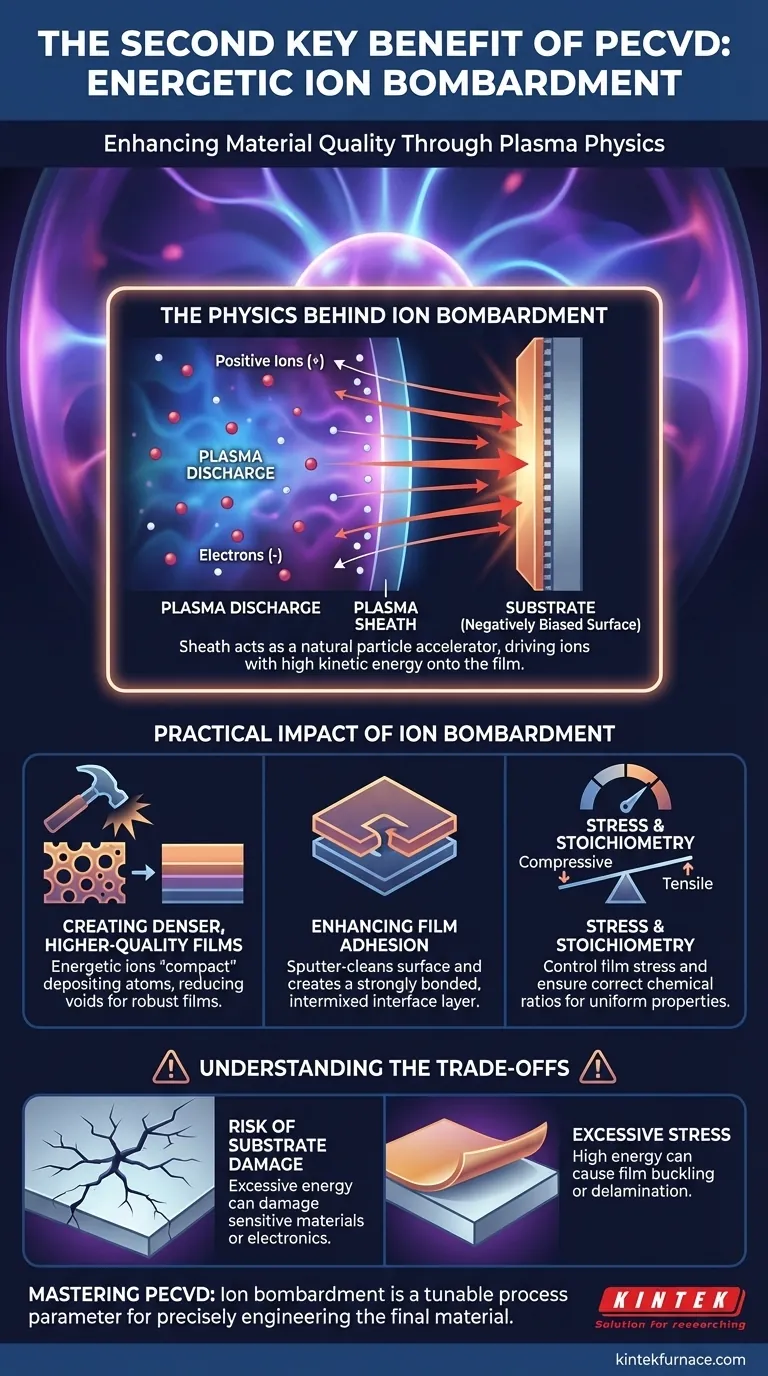
The Physics Behind Ion Bombardment
To understand why this bombardment occurs and why it's beneficial, we must look at the fundamental properties of a plasma discharge.
The Formation of the Plasma Sheath
In any plasma, electrons are thousands of times lighter and far more mobile than the heavy, slow-moving positive ions. As a result, electrons are initially lost to the substrate and chamber walls much faster than ions are.
This leaves the bulk of the plasma with a net positive charge relative to any surface it contacts. The resulting voltage difference is concentrated across a very thin boundary layer on the surface, known as the plasma sheath.
Ion Acceleration Across the Sheath
This sheath acts like a small, natural particle accelerator. The strong electric field within the sheath grabs positive ions from the edge of the plasma and accelerates them toward the negatively biased surface of the substrate.
These ions gain significant energy during this transit and strike the surface with high kinetic energy. This process is the energetic ion bombardment that defines the second major benefit of PECVD.
The Practical Impact of Ion Bombardment
This controlled bombardment during film growth provides several distinct advantages for the final material.
Creating Denser, Higher-Quality Films
In deposition processes without bombardment, atoms arrive at the surface with low energy and can arrange themselves in porous, low-density structures. Energetic ion bombardment acts like a microscopic hammer, "compacting" the depositing atoms and knocking them into more stable, denser configurations. This reduces voids and defects, leading to a higher-quality, more robust film.
Enhancing Film Adhesion
The ion energy serves two functions for adhesion. First, it can sputter-clean the substrate surface on an atomic scale just before deposition begins, removing contaminants. Second, the impact can slightly implant the first few layers of depositing atoms into the substrate, creating a strongly bonded, intermixed interface layer that dramatically improves adhesion.
Controlling Film Stress and Stoichiometry
By carefully tuning the plasma parameters—such as power, pressure, and gas mixture—an operator can control the energy of the bombarding ions. This provides a powerful lever for influencing intrinsic film properties like compressive or tensile stress. It also ensures enough energy is available to form highly uniform, stoichiometric films, where the elements are present in the correct chemical ratios.
Understanding the Trade-offs
While powerful, ion bombardment is not a universally positive effect. It must be carefully managed to avoid negative consequences.
The Risk of Substrate Damage
If the ion energy is too high, the bombardment can become destructive. It can create crystalline defects, amorphize the surface, or otherwise damage the underlying substrate. This is a critical concern when depositing on sensitive materials like polymers or delicate electronic devices.
The Problem of Excessive Stress
While bombardment helps control stress, excessive energy often leads to very high compressive stress within the film. This internal pressure can cause the film to buckle or even delaminate (peel off) from the substrate, representing a common failure mode in PECVD processes. The goal is always to find a balance.
Making the Right Choice for Your Goal
Effectively using PECVD requires treating ion bombardment not as an unavoidable side effect, but as a tunable process parameter.
- If your primary focus is high-quality, dense coatings: You will want to operate in a regime with moderate ion energy to ensure film compaction and good adhesion without causing damage.
- If your primary focus is depositing on sensitive or delicate substrates: Your goal is to minimize ion bombardment by using lower power settings or higher process pressures, even if it compromises deposition rate or density.
- If your primary focus is maximum deposition rate: You will increase plasma power and precursor gas flow, but you must carefully monitor film stress to find the upper limit before the bombardment energy causes film failure.
Ultimately, mastering PECVD means understanding and controlling this ion bombardment to precisely engineer the final material.
Summary Table:
| Benefit Aspect | Key Impact |
|---|---|
| Film Density | Reduces voids, creates denser structures |
| Adhesion | Cleans substrate, strengthens interface bonding |
| Stress Control | Allows tuning of compressive or tensile stress |
| Stoichiometry | Ensures uniform, correct chemical ratios in films |
| Trade-offs | Risk of substrate damage or excessive stress if not managed |
Unlock the full potential of PECVD for your lab with KINTEK! Leveraging exceptional R&D and in-house manufacturing, we provide advanced high-temperature furnace solutions tailored to your needs. Our product line includes Muffle, Tube, Rotary Furnaces, Vacuum & Atmosphere Furnaces, and CVD/PECVD Systems, all backed by strong deep customization capabilities to precisely meet your unique experimental requirements. Whether you're aiming for high-density coatings, delicate substrate handling, or optimized deposition rates, KINTEK delivers reliable, high-performance solutions. Contact us today to discuss how we can enhance your research and production processes!
Visual Guide
Related Products
- Slide PECVD Tube Furnace with Liquid Gasifier PECVD Machine
- RF PECVD System Radio Frequency Plasma Enhanced Chemical Vapor Deposition
- Inclined Rotary Plasma Enhanced Chemical Deposition PECVD Tube Furnace Machine
- Inclined Rotary Plasma Enhanced Chemical Deposition PECVD Tube Furnace Machine
- Multi Heating Zones CVD Tube Furnace Machine for Chemical Vapor Deposition Equipment
People Also Ask
- What are the main advantages of PECVD tube furnaces compared to CVD tube furnaces? Lower Temp, Faster Deposition, and More
- What are the disadvantages of tube furnace cracking when processing heavy raw materials? Avoid Costly Downtime and Inefficiency
- In which industries is the tube furnace commonly used? Essential for Materials Science, Energy, and More
- What role does a Tube Furnace play in the CVD growth of carbon nanotubes? Achieve High-Purity CNT Synthesis
- What are the advantages of using a tube furnace CVD system for Cu(111)/graphene? Superior Scalability and Quality


