At its core, Plasma-Enhanced Chemical Vapor Deposition (PECVD) is a thin film deposition process that differs from traditional Chemical Vapor Deposition (CVD) in one critical way. While conventional CVD relies exclusively on high thermal energy to drive chemical reactions, PECVD uses an energized plasma to achieve the same goal at significantly lower temperatures. This allows for the deposition of high-quality films on materials that cannot withstand the intense heat of traditional CVD.
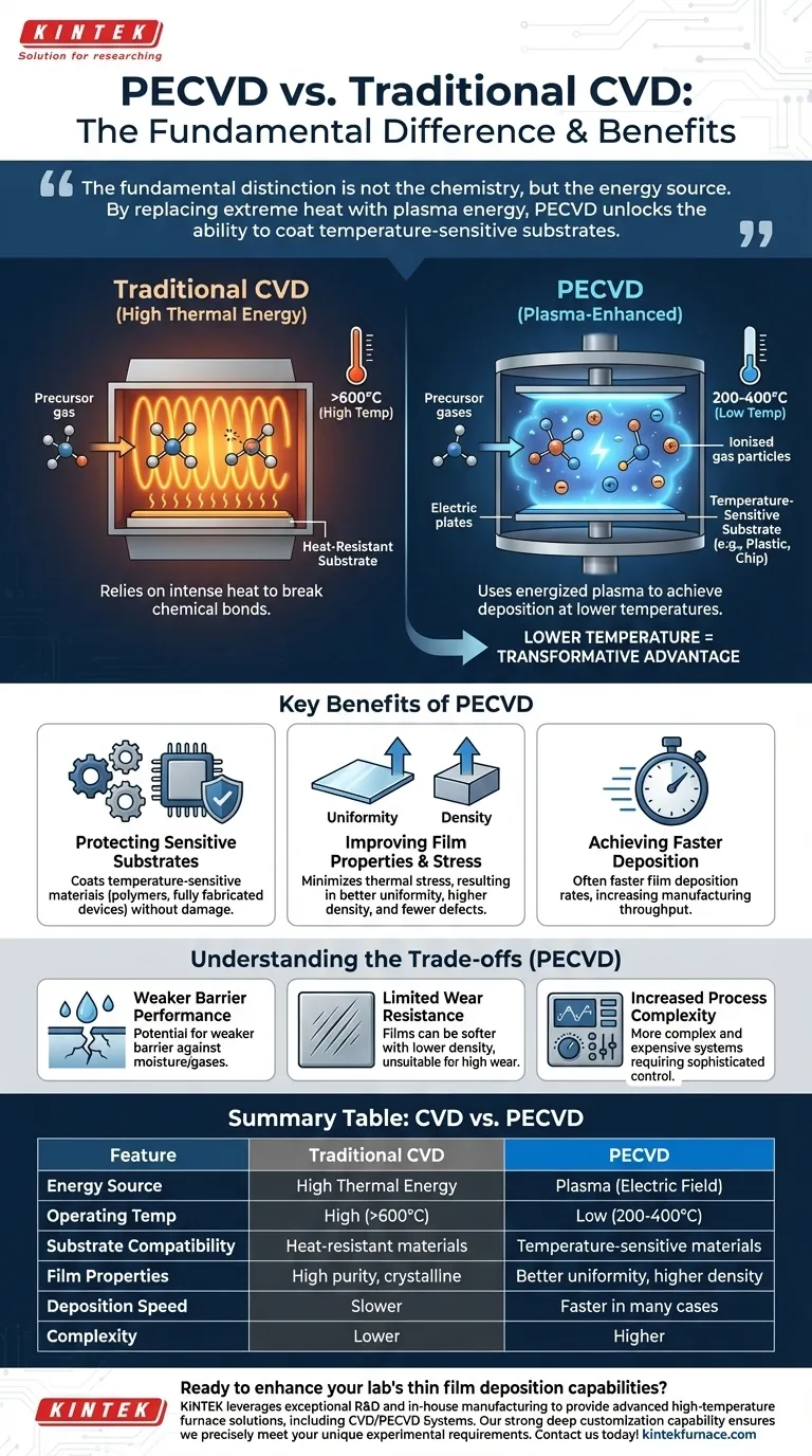
The fundamental distinction is not the chemistry, but the energy source. By replacing extreme heat with plasma energy, PECVD unlocks the ability to coat temperature-sensitive substrates, fundamentally expanding the applications of vapor deposition technology.
The Fundamental Difference: Energy Source
To understand the practical implications, you must first grasp how each process energizes the precursor gases to create a solid film.
Traditional CVD: Relying on Heat
Traditional CVD is conceptually simple. Precursor gases are introduced into a high-temperature furnace containing the substrate. The intense heat provides the thermal energy needed to break the chemical bonds in the gases, allowing them to react and deposit as a thin film onto the substrate surface.
This method is effective but its reliance on heat is also its primary limitation. Temperatures are often very high, which can damage or destroy many types of substrates.
PECVD: Introducing Plasma
PECVD adds a crucial element: an electric field that ionizes the precursor gases, creating a plasma. This plasma is a highly energetic state of matter containing ions and free electrons.
The energy within the plasma—not high temperature—is what breaks down the precursor molecules. This allows the deposition process to occur at much lower temperatures, typically in the 200-400°C range, and sometimes even lower.
How Lower Temperature Changes Everything
The ability to operate at lower temperatures is not a minor tweak; it is a transformative advantage with several critical benefits.
Protecting Temperature-Sensitive Substrates
This is the most significant advantage of PECVD. It enables the deposition of films on materials that would be destroyed by the heat of traditional CVD, such as plastics, polymers, and fully fabricated semiconductor devices with existing circuitry.
Improving Film Properties and Stress
High temperatures create thermal stress between the film and the substrate due to different rates of thermal expansion. PECVD minimizes this stress.
The result is often a film with better uniformity, higher density, and fewer defects like pinholes. This is crucial for creating reliable electronic and optical components.
Achieving Faster Deposition Speeds
In many industrial applications, such as chip fabrication, PECVD can achieve faster film deposition rates compared to thermal CVD. This directly translates to higher manufacturing throughput and efficiency.
Understanding the Trade-offs
While powerful, PECVD is not a universal solution. It comes with its own set of considerations and potential downsides.
Weaker Barrier Performance
Depending on the specific plasma conditions and materials used, PECVD films may exhibit weaker performance as a barrier against moisture or gases compared to films deposited by other methods.
Limited Wear Resistance
The lower-temperature process can sometimes result in films that are softer or have lower density than their high-temperature CVD counterparts. This can make them less suitable for applications requiring high wear resistance.
Increased Process Complexity
PECVD systems are more complex and expensive than simple thermal CVD furnaces. Managing the plasma requires sophisticated control over gas flow, pressure, and RF power, adding another layer of operational variables.
Making the Right Choice: CVD vs. PECVD
Choosing between these methods requires a clear understanding of your project's constraints and goals.
- If your primary focus is depositing a highly pure, crystalline film and your substrate can tolerate high heat: Traditional CVD is a robust, well-understood, and effective choice.
- If your primary focus is coating a temperature-sensitive substrate or minimizing thermal stress on your component: PECVD is the definitive and superior method, offering high-quality films without the risk of thermal damage.
Ultimately, understanding the role of energy—thermal versus plasma—is the key to selecting the right deposition technique for your specific application.
Summary Table:
| Feature | Traditional CVD | PECVD |
|---|---|---|
| Energy Source | High thermal energy | Plasma (electric field) |
| Operating Temperature | High (often >600°C) | Low (200-400°C) |
| Substrate Compatibility | Heat-resistant materials | Temperature-sensitive materials (e.g., plastics, semiconductors) |
| Film Properties | High purity, crystalline | Better uniformity, higher density, fewer defects |
| Deposition Speed | Slower | Faster in many cases |
| Complexity | Lower | Higher (requires plasma control) |
Ready to enhance your lab's thin film deposition capabilities? At KINTEK, we leverage exceptional R&D and in-house manufacturing to provide advanced high-temperature furnace solutions, including CVD/PECVD Systems. Our strong deep customization capability ensures we precisely meet your unique experimental requirements, whether you're working with temperature-sensitive substrates or need optimized film properties. Contact us today to discuss how our tailored solutions can drive your research and production forward!
Visual Guide
Related Products
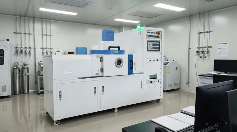
- Slide PECVD Tube Furnace with Liquid Gasifier PECVD Machine
- RF PECVD System Radio Frequency Plasma Enhanced Chemical Vapor Deposition
- Inclined Rotary Plasma Enhanced Chemical Deposition PECVD Tube Furnace Machine
- Inclined Rotary Plasma Enhanced Chemical Deposition PECVD Tube Furnace Machine
- Multi Heating Zones CVD Tube Furnace Machine for Chemical Vapor Deposition Equipment
People Also Ask
- What role does a Tube Furnace play in the CVD growth of carbon nanotubes? Achieve High-Purity CNT Synthesis
- What plasma source is used in PE-CVD tube furnaces? Unlock Low-Temperature, High-Quality Deposition
- How does PECVD equipment contribute to TOPCon bottom cells? Mastering Hydrogenation for Maximum Solar Efficiency
- What are the disadvantages of tube furnace cracking when processing heavy raw materials? Avoid Costly Downtime and Inefficiency
- What are the typical conditions for plasma-enhanced CVD processes? Achieve Low-Temperature Thin Film Deposition


