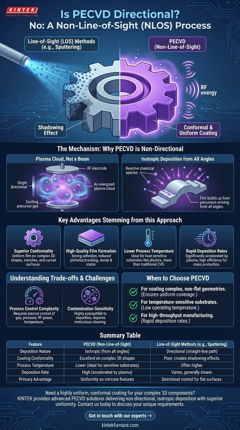
In short, no. Plasma-Enhanced Chemical Vapor Deposition (PECVD) is fundamentally a non-line-of-sight (NLOS) process. Unlike methods that fire a directional beam of particles at a target, PECVD creates a reactive plasma cloud that completely surrounds the substrate, allowing deposition to occur uniformly on all exposed surfaces from multiple angles.
The critical takeaway is that PECVD's non-directional nature is its core advantage. This characteristic allows it to produce highly uniform and conformal coatings on complex, three-dimensional shapes, a task that is inherently difficult for line-of-sight deposition techniques.
The Mechanism: Why PECVD is Non-Directional
The Role of Plasma, Not a Beam
Instead of a directional source, PECVD uses radio frequency (RF) energy to excite precursor gases into a reactive state known as plasma.
This plasma is a diffuse, energized gas cloud that fills the entire vacuum chamber, enveloping the substrate.
Isotropic Deposition from a Gas Cloud
The reactive chemical species within the plasma move in all directions and can land on any surface they contact.
This isotropic (uniform in all directions) nature of the deposition process is what makes it non-line-of-sight. The film builds up from precursors arriving from all angles, not from a single, direct path.
The Contrast with Line-of-Sight (LOS) Methods
Processes like filtered cathodic vacuum arc (FCVA), sputtering, or thermal evaporation are line-of-sight. They function like a spray paint can, where the material travels in a straight line from the source to the substrate.
This creates a "shadowing" effect, where surfaces not directly facing the source receive little or no coating. PECVD's plasma-based method effectively eliminates this problem.
Key Advantages Stemming from this Approach
Superior Conformality and Uniformity
The most significant benefit of PECVD's NLOS nature is its ability to coat complex geometries and 3D parts with a highly uniform and conformal film.
The plasma cloud ensures that even intricate trenches, steps, and curved surfaces are coated evenly, a key requirement in semiconductor and MEMS fabrication.
High-Quality Film Formation
The resulting films exhibit excellent properties. They have strong adhesion to the substrate and show a reduced likelihood of pinholes or cracking compared to other methods.
The plasma-enhanced reactions create a dense, stable film with high solvent and corrosion resistance.
Lower Process Temperature
The energy required for the chemical reactions comes from the excited plasma, not from high heat.
This allows deposition to occur at much lower temperatures than traditional Chemical Vapor Deposition (CVD), making PECVD ideal for temperature-sensitive substrates like plastics or pre-processed semiconductor wafers.
Rapid Deposition Rates
The plasma significantly accelerates the chemical reactions. This allows for high deposition rates—in some cases, over 100 times faster than conventional CVD—making PECVD highly efficient for mass production.
Understanding the Trade-offs and Challenges
Process Control Complexity
The main limitation of PECVD is the challenge of maintaining stable and reproducible conditions.
Achieving consistent results requires extremely precise control over numerous parameters, including gas flow rates, chamber pressure, RF power, and substrate temperature.
Contamination Sensitivity
The process is highly susceptible to contamination. Any residual gases or impurities within the chamber can be incorporated into the film, negatively impacting its quality and performance. Meticulous chamber cleaning and vacuum integrity are critical.
When to Choose PECVD
Choosing a deposition method depends entirely on your project's specific requirements. PECVD is not a universal solution, but it excels in specific scenarios.
- If your primary focus is coating complex, non-flat geometries: PECVD is an excellent choice due to its non-line-of-sight nature, which ensures uniform and conformal coverage.
- If your primary focus is depositing on temperature-sensitive substrates: The low operating temperature of PECVD makes it significantly advantageous over high-temperature thermal CVD processes.
- If your primary focus is high-throughput manufacturing: The rapid deposition rates of PECVD can accelerate production cycles for materials like silicon nitride and silicon dioxide without sacrificing film quality.
Understanding that PECVD's power lies in its non-directional nature is the key to leveraging it effectively for your technical goals.
Summary Table:
| Feature | PECVD (Non-Line-of-Sight) | Line-of-Sight Methods (e.g., Sputtering) |
|---|---|---|
| Deposition Nature | Isotropic (from all angles) | Directional (straight-line path) |
| Coating Conformality | Excellent on complex 3D shapes | Poor; creates shadowing effects |
| Process Temperature | Lower (ideal for sensitive substrates) | Often higher |
| Deposition Rate | High (accelerated by plasma) | Varies, generally slower |
| Primary Advantage | Uniformity on intricate features | Directional control for flat surfaces |
Need a highly uniform, conformal coating for your complex 3D components?
Leveraging exceptional R&D and in-house manufacturing, KINTEK provides diverse laboratories with advanced PECVD solutions. Our systems are designed to deliver the non-directional, isotropic deposition essential for coating intricate geometries, trenches, and temperature-sensitive substrates with superior uniformity and adhesion.
Contact us today to discuss how our deep customization capabilities can precisely meet your unique experimental or production requirements.
Get in touch with our experts →
Visual Guide
Related Products
- Slide PECVD Tube Furnace with Liquid Gasifier PECVD Machine
- RF PECVD System Radio Frequency Plasma Enhanced Chemical Vapor Deposition
- Inclined Rotary Plasma Enhanced Chemical Deposition PECVD Tube Furnace Machine
- Inclined Rotary Plasma Enhanced Chemical Deposition PECVD Tube Furnace Machine
- Multi Heating Zones CVD Tube Furnace Machine for Chemical Vapor Deposition Equipment
People Also Ask
- What are the advantages of using a tube furnace CVD system for Cu(111)/graphene? Superior Scalability and Quality
- What are the disadvantages of tube furnace cracking when processing heavy raw materials? Avoid Costly Downtime and Inefficiency
- In which industries is the tube furnace commonly used? Essential for Materials Science, Energy, and More
- What is plasma in the context of PECVD? Unlock Low-Temperature Thin Film Deposition
- What plasma source is used in PE-CVD tube furnaces? Unlock Low-Temperature, High-Quality Deposition


