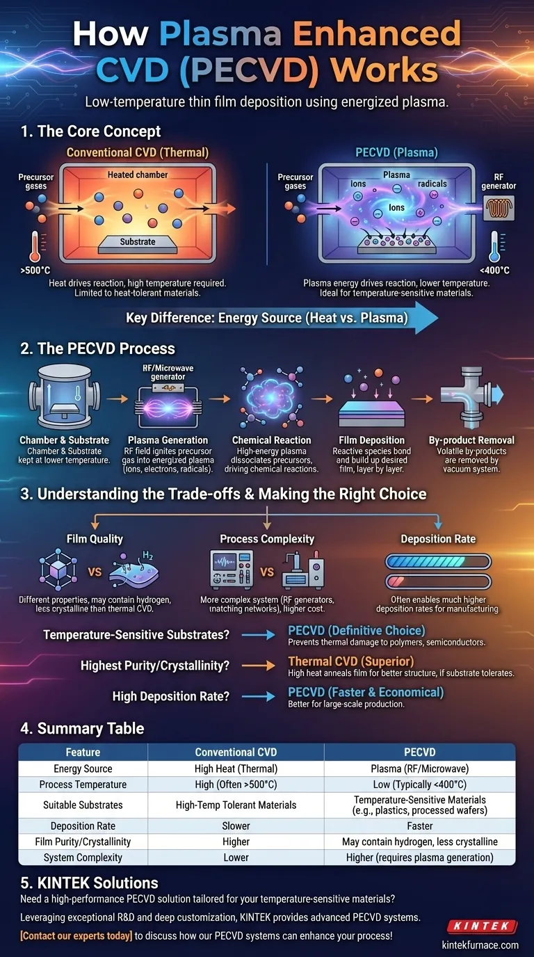
At its core, Plasma Enhanced Chemical Vapor Deposition (PECVD) is a process for creating thin films on a substrate. Unlike traditional methods that rely on extreme heat, PECVD uses the energy of a plasma to initiate the chemical reactions needed for deposition. This allows for high-quality coatings to be applied at significantly lower temperatures.
The crucial difference between PECVD and conventional Chemical Vapor Deposition (CVD) is its energy source. By using an energized plasma instead of high heat to break down precursor gases, PECVD enables the coating of temperature-sensitive materials that would otherwise be damaged or destroyed.
The Foundation: Understanding Conventional CVD
To appreciate what makes PECVD unique, it's essential first to understand the conventional thermal CVD process it evolved from.
The Role of Heat and Precursors
In thermal CVD, a substrate is placed inside a vacuum chamber which is then heated to a very high temperature. Precursor gases containing the elements of the desired film are then introduced into this hot chamber.
The Deposition Process
The intense heat provides the energy needed to break down the precursor gas molecules. These decomposed elements then react and deposit onto the cooler substrate, gradually building up a thin, uniform layer of solid material.
The Key Limitation: Temperature
The primary drawback of thermal CVD is its reliance on extreme temperatures, often many hundreds of degrees Celsius. This requirement makes it unsuitable for coating materials with low melting points, such as plastics, or delicate electronic components.
The PECVD Difference: Introducing Plasma
PECVD was developed specifically to overcome the temperature limitations of thermal CVD. It achieves this by fundamentally changing how energy is delivered to the system.
What is Plasma?
Plasma is often called the "fourth state of matter." It is a gas that has been energized—typically by a radio frequency (RF) or microwave field—to the point where its atoms are broken apart into a mixture of ions, electrons, and highly reactive free radicals.
How Plasma Replaces High Heat
In a PECVD process, the chamber and substrate are kept at a much lower temperature. Instead of heat, an electric field is used to ignite the precursor gases into a plasma.
The immense energy contained within this plasma is what drives the chemical reactions. The highly reactive species in the plasma break down the precursor molecules far more efficiently than heat alone.
The Deposition Mechanism
Once the precursor gases are dissociated into reactive fragments within the plasma, they travel to the substrate surface. There, they bond and build up the desired thin film, layer by layer. The volatile by-products are then removed by the vacuum system.
Understanding the Trade-offs
While the low-temperature advantage is significant, choosing PECVD involves considering certain trade-offs inherent to the process.
Film Quality and Composition
Because the chemical reactions in PECVD are driven by plasma rather than thermal equilibrium, the resulting films can have different properties. For instance, films may have hydrogen incorporated into their structure, which can be either a benefit or a drawback depending on the application.
Process Complexity
A PECVD system is more complex than a basic thermal CVD reactor. It requires sophisticated RF or microwave power generators and matching networks to create and sustain a stable plasma, adding to the cost and operational difficulty.
Deposition Rate vs. Control
PECVD often enables much higher deposition rates than thermal CVD, which is a major industrial advantage. However, the plasma adds more variables to the process (power, pressure, gas flow), which can make fine-tuning film properties like uniformity and stress more challenging.
Making the Right Choice for Your Goal
Selecting the correct deposition method requires matching the process capabilities to your project's most critical requirement.
- If your primary focus is coating temperature-sensitive substrates: PECVD is the definitive choice, as its low-temperature operation prevents thermal damage to materials like polymers or pre-processed semiconductor wafers.
- If your primary focus is achieving the highest film purity or crystallinity: Thermal CVD is often superior, as the high processing temperatures can anneal the film as it grows, leading to a more ordered structure, provided your substrate can tolerate the heat.
- If your primary focus is a high deposition rate for manufacturing: PECVD is generally faster and more economical for large-scale production, especially when the absolute highest film purity is not the main driver.
Ultimately, understanding that the energy source—plasma versus heat—dictates the entire process window is the key to selecting the right technology.
Summary Table:
| Feature | Conventional CVD | PECVD |
|---|---|---|
| Energy Source | High Heat (Thermal) | Plasma (RF/Microwave) |
| Process Temperature | High (Often >500°C) | Low (Typically <400°C) |
| Suitable Substrates | High-Temp Tolerant Materials | Temperature-Sensitive Materials (e.g., plastics, processed wafers) |
| Deposition Rate | Slower | Faster |
| Film Purity/Crystallinity | Higher | May contain hydrogen, less crystalline |
| System Complexity | Lower | Higher (requires plasma generation) |
Need a high-performance PECVD solution tailored for your temperature-sensitive materials?
Leveraging exceptional R&D and in-house manufacturing, KINTEK provides diverse laboratories with advanced high-temperature furnace solutions. Our product line, including PECVD Systems, is complemented by our strong deep customization capability to precisely meet unique experimental requirements.
Contact our experts today to discuss how our PECVD systems can enhance your thin film deposition process!
Visual Guide
Related Products
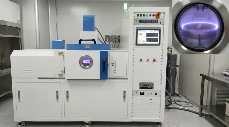
- RF PECVD System Radio Frequency Plasma Enhanced Chemical Vapor Deposition
- Slide PECVD Tube Furnace with Liquid Gasifier PECVD Machine
- Inclined Rotary Plasma Enhanced Chemical Deposition PECVD Tube Furnace Machine
- Inclined Rotary Plasma Enhanced Chemical Deposition PECVD Tube Furnace Machine
- MPCVD Machine System Reactor Bell-jar Resonator for Lab and Diamond Growth
People Also Ask
- How is silicon dioxide deposited from tetraethylorthosilicate (TEOS) in PECVD? Achieve Low-Temperature, High-Quality SiO2 Films
- How are deposition rates and film properties controlled in PECVD? Master Key Parameters for Optimal Thin Films
- What are the advantages of PECVD in film deposition? Achieve Low-Temp, High-Quality Coatings
- What is RF in PECVD? A Critical Control for Plasma Deposition
- How does film quality compare between PECVD and CVD? Choose the Best Method for Your Substrate