In short, Plasma-Enhanced Chemical Vapor Deposition (PECVD) is a foundational technology for manufacturing advanced optical coatings. It enables the deposition of thin films with precisely engineered optical properties—such as a specific refractive index—onto a wide variety of materials, including those that cannot withstand high heat. This control makes it essential for creating products like anti-reflective lenses, specialized mirrors, and optical filters.
The true advantage of PECVD in optics is not just its ability to deposit a coating, but its power to do so at low temperatures. This unlocks the use of high-performance optical coatings on heat-sensitive materials like plastics and allows for uniform coverage on complex, non-flat surfaces.
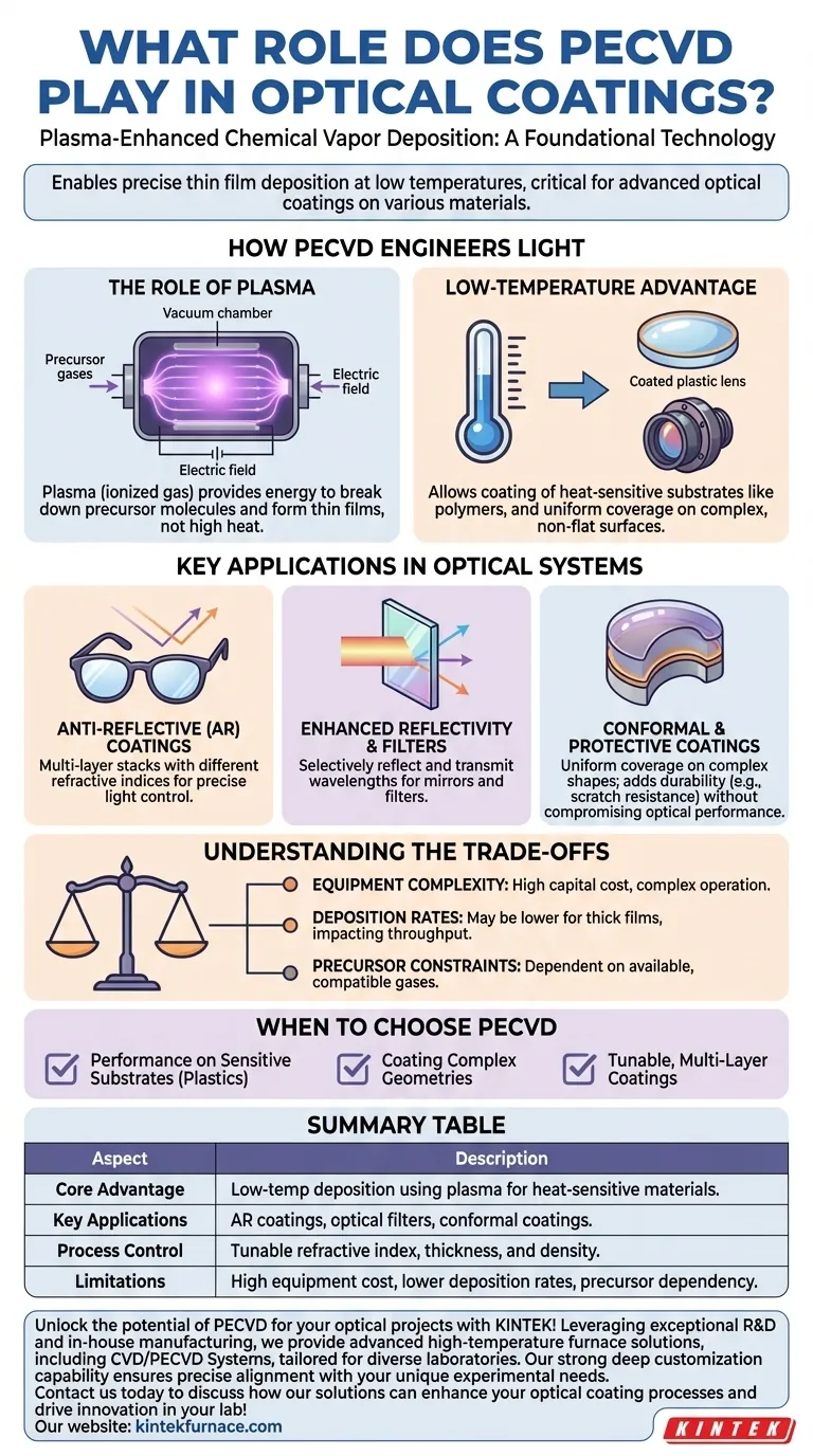
How PECVD Engineers Light
The effectiveness of PECVD stems from its unique method of energizing the deposition process. Unlike traditional Chemical Vapor Deposition (CVD), which relies on high temperatures, PECVD uses plasma.
The Role of Plasma
The process takes place in a vacuum chamber where precursor gases are introduced. An electric field is applied, exciting the gas into a plasma—an ionized state of matter.
This plasma contains highly reactive ions and radicals. It provides the necessary energy to break down the precursor molecules and drive the chemical reactions that form the thin film on the substrate's surface.
The Low-Temperature Advantage
Because the plasma provides the energy, the substrate itself does not need to be heated to extreme temperatures. This is the single most important advantage for many optical applications.
This allows for the successful coating of temperature-sensitive substrates like polymers (plastics), assembled optical components, and other materials that would be damaged or destroyed by high-temperature deposition methods.
Precision Through Process Control
The final properties of the optical coating are directly tied to the process parameters. By meticulously controlling the gas composition, pressure, temperature, and plasma power, engineers can precisely tune the film's characteristics.
Most critically, this allows for the fine-tuning of the refractive index, density, and thickness of the film, which are the fundamental variables used to control how light reflects from or transmits through a surface.
Key Applications in Optical Systems
PECVD's control and low-temperature processing enable a range of critical optical applications.
Anti-Reflective (AR) Coatings
AR coatings reduce unwanted reflections from surfaces like eyeglass lenses and camera optics. They typically consist of multiple layers, each with a different refractive index and thickness.
PECVD is ideal for creating these complex multi-layer stacks, as it allows for the precise, sequential deposition of different materials to achieve the desired destructive interference of light waves.
Enhanced Reflectivity and Filters
The same principle of layering materials with different refractive indices can be used to create highly reflective coatings for mirrors or specialized optical filters.
These filters, known as dichroic filters, are designed to selectively reflect certain wavelengths of light while transmitting others, a capability essential in devices like photometers and projection systems.
Conformal and Protective Coatings
PECVD provides excellent conformal coverage, meaning it can deposit a uniform film over parts with complex or irregular shapes, such as curved lenses or intricate optical sensors.
Furthermore, it can be used to deposit hard, durable materials like silicon nitride. These films add scratch resistance and environmental protection to delicate optical surfaces without compromising their optical performance.
Understanding the Trade-offs
While powerful, PECVD is not a universal solution. An objective assessment requires understanding its limitations.
Equipment and Process Complexity
PECVD systems are complex vacuum chambers that require significant capital investment and expertise to operate and maintain. The process itself can be sensitive to contamination and requires careful calibration.
Deposition Rates
While effective, PECVD can have lower deposition rates compared to some other methods like sputtering. For applications requiring very thick films, this can lead to longer processing times, impacting throughput and cost.
Precursor Material Constraints
The process is dependent on the availability of suitable precursor gases that can be effectively dissociated in a plasma to form the desired film. The chemistry must be compatible with the plasma environment, and precursor purity is critical to the quality of the final optical coating.
When to Choose PECVD for Your Optical Project
Your choice of deposition technology depends entirely on your project's specific constraints and performance goals.
- If your primary focus is performance on sensitive substrates: PECVD is the definitive choice for coating plastics, polymers, or pre-assembled components that cannot tolerate high heat.
- If your primary focus is coating complex geometries: The conformal nature of PECVD makes it superior for achieving uniform coatings on curved lenses, structured optics, or other non-flat surfaces.
- If your primary focus is tunable, multi-layer coatings: PECVD provides the layer-by-layer control over refractive index and thickness required for high-performance AR coatings and advanced optical filters.
By understanding its core mechanism and trade-offs, you can confidently determine if PECVD is the right tool to achieve your specific optical goals.
Summary Table:
| Aspect | Description |
|---|---|
| Core Advantage | Low-temperature deposition using plasma, enabling coating of heat-sensitive materials like plastics. |
| Key Applications | Anti-reflective coatings, optical filters, conformal coatings on complex shapes. |
| Process Control | Tunable refractive index, thickness, and density through gas, pressure, and plasma power adjustments. |
| Limitations | High equipment cost, lower deposition rates, and dependency on precursor gases. |
Unlock the potential of PECVD for your optical projects with KINTEK! Leveraging exceptional R&D and in-house manufacturing, we provide advanced high-temperature furnace solutions, including CVD/PECVD Systems, tailored for diverse laboratories. Our strong deep customization capability ensures precise alignment with your unique experimental needs, whether you're developing anti-reflective coatings, optical filters, or coatings on heat-sensitive materials. Contact us today to discuss how our solutions can enhance your optical coating processes and drive innovation in your lab!
Visual Guide
Related Products
- RF PECVD System Radio Frequency Plasma Enhanced Chemical Vapor Deposition
- Inclined Rotary Plasma Enhanced Chemical Deposition PECVD Tube Furnace Machine
- Slide PECVD Tube Furnace with Liquid Gasifier PECVD Machine
- Inclined Rotary Plasma Enhanced Chemical Deposition PECVD Tube Furnace Machine
- HFCVD Machine System Equipment for Drawing Die Nano Diamond Coating
People Also Ask
- How does film quality compare between PECVD and CVD? Choose the Best Method for Your Substrate
- What is RF in PECVD? A Critical Control for Plasma Deposition
- What are the key advantages of PECVD technology? Achieve Low-Temperature, High-Quality Thin Film Deposition
- What is the role of RF power in PECVD and how does the RF-PECVD process work? Master Thin Film Deposition Control
- How is silicon dioxide deposited from tetraethylorthosilicate (TEOS) in PECVD? Achieve Low-Temperature, High-Quality SiO2 Films


