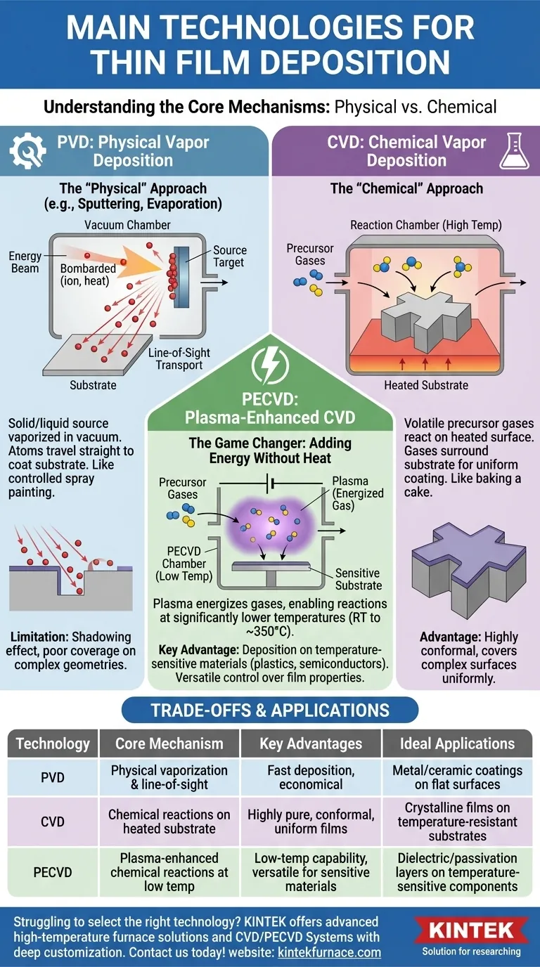
At its core, thin film deposition is accomplished through two primary families of technology: Physical Vapor Deposition (PVD) and Chemical Vapor Deposition (CVD). PVD involves physically transporting material from a source to your substrate, while CVD uses chemical reactions from precursor gases to grow a film directly on the substrate's surface. A critical variant, Plasma-Enhanced Chemical Vapor Deposition (PECVD), uses plasma to enable these chemical reactions at much lower temperatures.
The fundamental choice between deposition technologies is not about which is "better," but about matching the process to the material and the substrate. The decision hinges on a trade-off between the physical "line-of-sight" nature of PVD and the chemical "conformal" nature of CVD, along with the temperature tolerance of your components.
The Two Pillars of Deposition: PVD vs. CVD
Understanding the foundational difference between physical and chemical deposition is the first step toward choosing the right technology. They build films in fundamentally distinct ways.
Physical Vapor Deposition (PVD): The "Physical" Approach
PVD encompasses a set of vacuum deposition methods where a solid or liquid source material is vaporized in a vacuum environment and then transported atom-by-atom to the substrate.
Think of it as a highly controlled form of spray painting. A source "target" is bombarded with energy (like an ion beam in sputtering) or heated (in evaporation), which ejects atoms that travel in a straight line until they hit the substrate and condense into a film.
This line-of-sight travel is a defining characteristic of PVD.
Chemical Vapor Deposition (CVD): The "Chemical" Approach
CVD involves introducing one or more volatile precursor gases into a reaction chamber. These gases decompose or react on the heated substrate's surface to produce the desired solid film.
This process is more like baking. The ingredients (gases) are mixed in an oven (the chamber), and the heat on the pan's surface (the substrate) causes them to react and form a solid cake (the thin film).
Because the gas molecules surround the substrate, CVD is known for producing highly conformal coatings that cover complex, three-dimensional surfaces uniformly.
The Game Changer: Plasma-Enhanced CVD (PECVD)
Traditional CVD often requires very high temperatures (hundreds or even over 1000°C) to drive the necessary chemical reactions. PECVD was developed to overcome this critical limitation.
How PECVD Works: Adding Energy Without Heat
PECVD uses an electric field to generate a plasma (an energized gas) within the reaction chamber.
This plasma transfers energy to the precursor gas molecules, allowing them to react and form a film at significantly lower temperatures—often from room temperature to around 350°C.
The Key Advantages of PECVD
This low-temperature capability makes PECVD exceptionally versatile. It allows for the deposition of high-quality films on substrates that cannot withstand the heat of traditional CVD, such as plastics, certain semiconductors, and fully assembled devices.
As a result, PECVD offers excellent control over material properties like refractive index, film stress, and hardness, while maintaining good uniformity and step coverage.
Understanding the Trade-offs: Which Process for Which Goal?
There is no single best technology; each has inherent strengths and weaknesses that make it suitable for different applications.
PVD: Speed vs. Coverage
PVD is often preferred for depositing metals and other simple compounds on relatively flat surfaces. Its primary limitation is the "shadowing effect" caused by its line-of-sight nature, leading to poor coverage in trenches or on complex geometries.
CVD: Quality vs. Temperature
Traditional CVD is the gold standard for creating extremely pure, dense, and highly uniform crystalline films. Its main drawback is the high process temperature, which limits the types of substrates it can be used on.
PECVD: Versatility vs. Complexity
PECVD solves the temperature problem of CVD, enabling high-quality, conformal films on sensitive substrates. However, the plasma process can sometimes introduce hydrogen or other impurities into the film and can be more complex to control than PVD or thermal CVD.
Making the Right Choice for Your Application
Your final decision should be guided by your primary objective for the thin film.
- If your primary focus is depositing a simple metallic or ceramic coating on a flat surface: PVD is often the most direct, economical, and fastest choice.
- If your primary focus is growing a highly pure, crystalline film on a temperature-resistant substrate: Traditional CVD offers unmatched film quality and conformity.
- If your primary focus is depositing a high-quality, conformal dielectric or passivation layer on a temperature-sensitive component: PECVD provides the best balance of performance and process flexibility.
Understanding the core mechanism—physical transport versus chemical reaction—is the key to navigating these technologies and selecting the optimal path for your project.
Summary Table:
| Technology | Core Mechanism | Key Advantages | Ideal Applications |
|---|---|---|---|
| PVD | Physical vaporization and line-of-sight transport | Fast deposition, economical for flat surfaces | Metal/ceramic coatings on flat substrates |
| CVD | Chemical reactions on heated substrate | Highly pure, conformal, uniform films | Crystalline films on temperature-resistant substrates |
| PECVD | Plasma-enhanced chemical reactions at low temperatures | Low-temperature capability, versatile for sensitive materials | Dielectric/passivation layers on temperature-sensitive components |
Struggling to select the right thin film deposition technology for your lab? At KINTEK, we leverage exceptional R&D and in-house manufacturing to provide advanced high-temperature furnace solutions tailored to your needs. Our product line—including Muffle, Tube, Rotary Furnaces, Vacuum & Atmosphere Furnaces, and CVD/PECVD Systems—is complemented by strong deep customization capabilities to precisely meet your unique experimental requirements. Contact us today to enhance your deposition processes and achieve superior results!
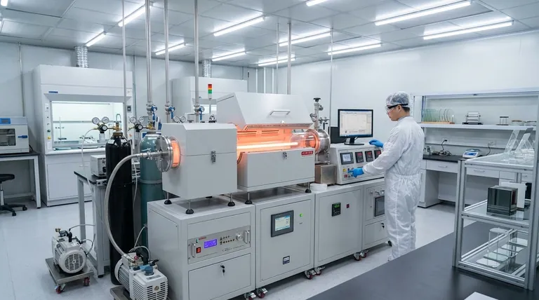
Visual Guide
Related Products
- HFCVD Machine System Equipment for Drawing Die Nano Diamond Coating
- RF PECVD System Radio Frequency Plasma Enhanced Chemical Vapor Deposition
- Slide PECVD Tube Furnace with Liquid Gasifier PECVD Machine
People Also Ask
- What is Hot-filament Chemical Vapor Deposition (HFCVD)? Achieve High-Quality Thin Films with Precision Control
- What is the advantage of using a CVD system for coating turbine blades? Master Complex Geometries with Ease
- What is the function of high-purity Argon (Ar) gas during CVD? Optimize Your Thin Film Uniformity and Purity
- What is the significance of the vacuum pressure control system in the CVD coating process for powders?
- What role does Chemical Vapor Deposition (CVD) equipment play in the surface coating of carbon fibers for composites?


