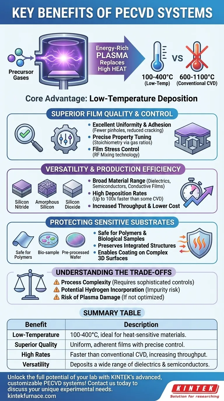
At its core, Plasma-Enhanced Chemical Vapor Deposition (PECVD) overcomes the primary limitation of conventional CVD by enabling high-quality film deposition at significantly lower temperatures. This is achieved by using an energy-rich plasma to break down precursor gases, replacing the need for high thermal energy. This fundamental difference makes PECVD an indispensable tool for depositing films on heat-sensitive substrates or devices that cannot tolerate high-temperature processing.
The central advantage of PECVD is its use of plasma to drive chemical reactions at low temperatures. This unlocks the ability to create high-quality, uniform, and precisely controlled thin films on a wide variety of materials without causing thermal damage.
The Core Advantage: Low-Temperature Deposition
The most significant benefit of PECVD is its low-temperature operation, often in the range of 100-400°C, compared to the 600-1100°C required for many conventional Chemical Vapor Deposition (CVD) processes.
How Plasma Replaces Heat
Instead of relying solely on thermal energy, PECVD systems generate a plasma—an ionized gas containing a mix of electrons, ions, and highly reactive neutral species. This plasma provides the energy needed to dissociate the precursor gas molecules and initiate the chemical reactions that form the thin film on the substrate surface.
This process effectively decouples the reaction energy from the substrate temperature.
Protecting Sensitive Substrates
The low process temperature is critical for applications involving materials that would be damaged or destroyed by the heat of traditional CVD. This includes depositing films onto polymers, biological samples, or semiconductor wafers that already have metallic layers or other temperature-sensitive integrated structures.
Achieving Superior Film Quality and Control
Beyond temperature, PECVD provides a high degree of control over the final properties of the deposited film, leading to superior performance and reliability.
High-Quality and Uniform Films
PECVD processes are known for producing films with excellent uniformity across the entire substrate. This is often aided by system designs like "showerhead" gas inlets, which distribute precursor gases evenly over the surface.
The resulting films have fewer pinholes and a reduced tendency to crack, leading to more robust and reliable device performance.
Excellent Adhesion and Coverage
The energetic plasma environment can enhance the adhesion of the deposited film to the substrate. Furthermore, PECVD is highly effective at coating complex, three-dimensional surfaces, offering better conformity than many line-of-sight deposition techniques like Physical Vapor Deposition (PVD).
Precise Control Over Film Properties
Operators can precisely tune the final film's characteristics by adjusting process parameters. For example, adjusting gas ratios allows for fine control over the film's stoichiometry (the exact chemical composition).
A key technique is the use of high and low-frequency RF mixing. By blending different radio frequencies to drive the plasma, engineers can directly manipulate and control the internal stress of the film, which is critical for preventing cracking or delamination.
Versatility and Production Efficiency
PECVD is not a niche technique; it is a versatile and efficient method used across a vast range of industrial and research applications.
A Broad Range of Materials
The process is remarkably versatile, capable of depositing a wide variety of materials. This includes dielectrics (like silicon nitride and silicon dioxide), semiconductors (like amorphous silicon), and even some conductive films.
High Deposition Rates
PECVD can achieve significantly faster deposition rates than many competing processes. For materials like silicon nitride, deposition can be over 100 times faster than with conventional low-pressure CVD, drastically increasing manufacturing throughput and reducing cost.
Understanding the Trade-offs
While powerful, PECVD is not without its complexities. A clear understanding of its limitations is essential for successful implementation.
Process Complexity
Controlling a plasma environment is inherently more complex than managing a purely thermal process. It requires sophisticated RF power delivery systems and advanced process controls to maintain stability and repeatability.
Potential for Contamination
Because the precursor gases often contain hydrogen (e.g., in silane, SiH₄), the resulting films can have hydrogen incorporated into them. While sometimes benign or even beneficial, this can be an undesirable impurity in high-performance electronic or optical applications.
Risk of Plasma Damage
The same energetic ions that drive the reaction can also cause physical damage to the substrate surface or the growing film if the process is not carefully optimized. This is a key consideration when working with extremely sensitive electronic devices.
Making the Right Choice for Your Application
Selecting the right deposition method depends entirely on your project's primary constraints and goals.
- If your primary focus is depositing on polymers or pre-processed wafers: PECVD is often the only viable choice due to its low-temperature capability.
- If your primary focus is high-throughput manufacturing: PECVD's high deposition rates offer a clear advantage for efficiency and cost-effectiveness.
- If your primary focus is preventing film cracking or delamination: PECVD provides unique control over film stress through techniques like dual-frequency RF mixing.
- If your primary focus is achieving the absolute highest film purity: You must consider the potential for hydrogen incorporation and evaluate if a higher-temperature CVD process might yield a purer, albeit more thermally expensive, result.
Ultimately, PECVD is a powerful and versatile deposition tool that expands what is possible in materials science and engineering.
Summary Table:
| Benefit | Description |
|---|---|
| Low-Temperature Deposition | Enables film deposition at 100-400°C, ideal for heat-sensitive materials like polymers and semiconductors. |
| Superior Film Quality | Produces uniform, adherent films with precise control over properties like stoichiometry and stress. |
| High Deposition Rates | Faster than conventional CVD, increasing throughput and reducing manufacturing costs. |
| Versatility | Deposits a wide range of materials including dielectrics, semiconductors, and conductive films. |
| Protection for Substrates | Prevents thermal damage, making it suitable for sensitive devices and complex 3D surfaces. |
Unlock the full potential of your lab with KINTEK's advanced PECVD systems! Leveraging exceptional R&D and in-house manufacturing, we provide diverse laboratories with tailored high-temperature furnace solutions, including PECVD systems designed for low-temperature, high-quality film deposition. Our strong deep customization capability ensures we precisely meet your unique experimental needs, enhancing efficiency and reliability. Contact us today to discuss how our PECVD systems can benefit your specific applications!
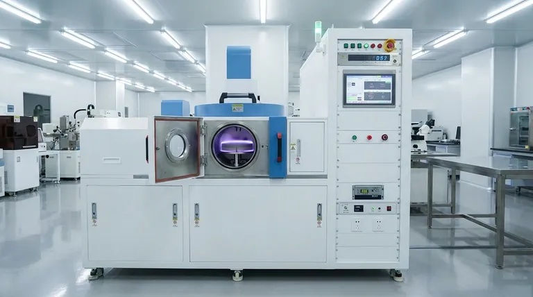
Visual Guide
Related Products
- RF PECVD System Radio Frequency Plasma Enhanced Chemical Vapor Deposition
- Slide PECVD Tube Furnace with Liquid Gasifier PECVD Machine
- Inclined Rotary Plasma Enhanced Chemical Deposition PECVD Tube Furnace Machine
- Inclined Rotary Plasma Enhanced Chemical Deposition PECVD Tube Furnace Machine
- Cylindrical Resonator MPCVD Machine System for Lab Diamond Growth
People Also Ask
- What are some promising applications of PECVD-prepared 2D materials? Unlock Advanced Sensing and Optoelectronics
- How is silicon dioxide deposited from tetraethylorthosilicate (TEOS) in PECVD? Achieve Low-Temperature, High-Quality SiO2 Films
- What is RF in PECVD? A Critical Control for Plasma Deposition
- How are deposition rates and film properties controlled in PECVD? Master Key Parameters for Optimal Thin Films
- How does film quality compare between PECVD and CVD? Choose the Best Method for Your Substrate


