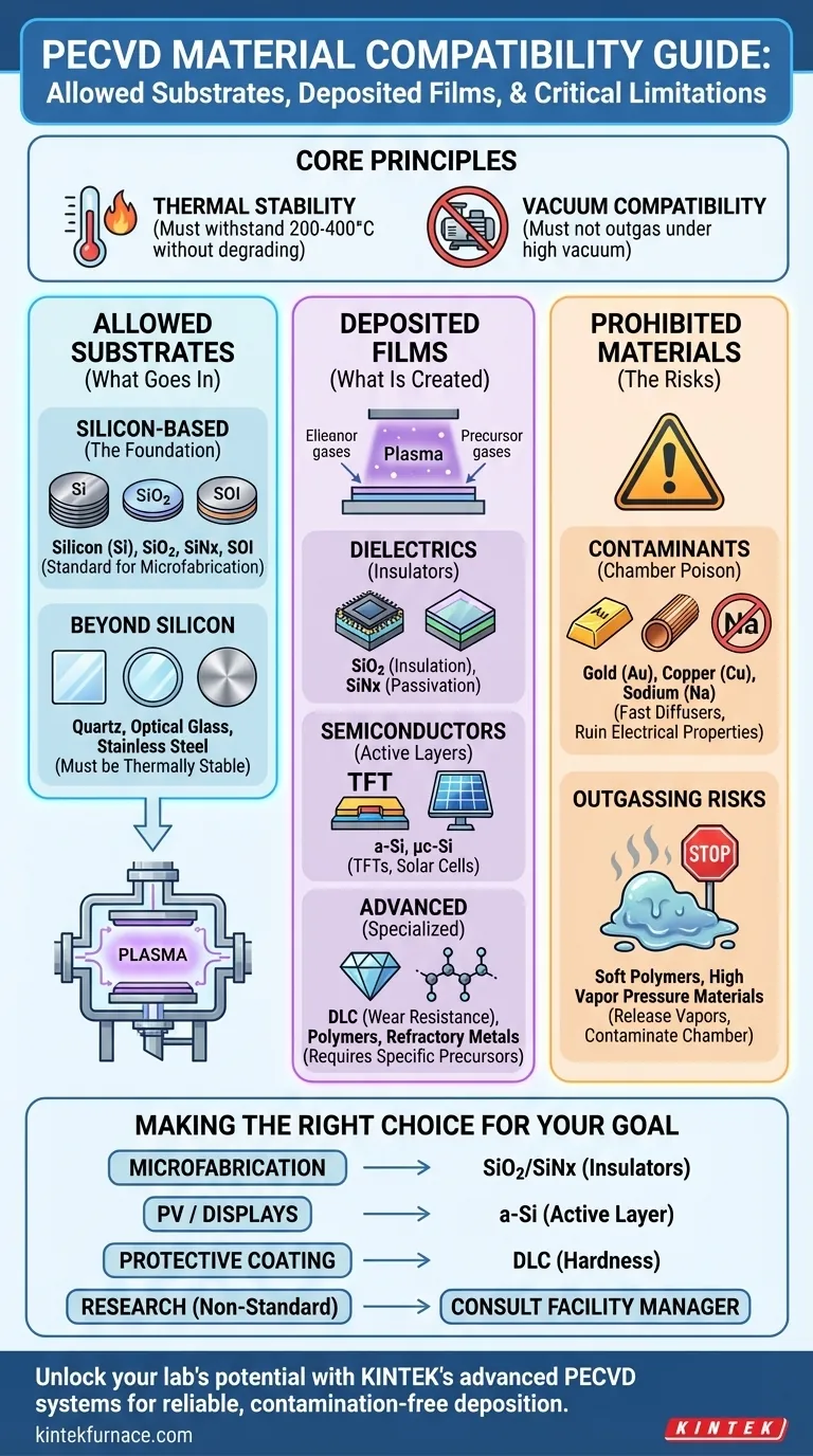
In short, a PECVD system allows substrates that are thermally stable and vacuum-compatible, such as silicon wafers, quartz, and certain glasses. The process itself is used to deposit a wide variety of thin films, with the most common being silicon nitride (SiNx), silicon dioxide (SiO2), and amorphous silicon (a-Si).
The core question isn't just what materials are allowed, but why. Material compatibility in a Plasma-Enhanced Chemical Vapor Deposition (PECVD) system is governed by two principles: the substrate must survive the process conditions without degrading, and the process chemistry must be compatible with the system to prevent chamber contamination.
Allowed Substrates: What Goes Inside the Chamber?
The material you place inside the chamber, known as the substrate, must withstand the process environment. The main constraints are its ability to handle moderate heat and high vacuum without releasing contaminants.
The Foundation: Silicon-Based Materials
The most common and universally accepted substrates are silicon-based. These include pure silicon (Si) wafers, wafers with thermally grown silicon dioxide (SiO2), wafers coated with silicon nitride (SixNy), and Silicon-on-Insulator (SOI) wafers.
These materials are the standard for semiconductor manufacturing and are inherently compatible with the chemistry used to deposit more silicon-based films.
Beyond Silicon: Glass, Quartz, and Metals
PECVD is not limited to silicon. Substrates like optical glass, quartz, and even some metals like stainless steel are often permissible.
The absolute requirement is that they are compatible with the process temperature, which is typically in the range of 200-400°C.
The Critical Rule: Thermal and Vacuum Stability
Any material placed in the chamber must be thermally stable at the deposition temperature. It cannot melt, deform, or—most importantly—outgas.
Outgassing is the release of trapped vapors from a material under vacuum, which can contaminate the process chamber and ruin the deposition for you and future users. This is why materials like soft polymers or anything with high vapor pressure are forbidden.
Deposited Films: What Can Be Created?
PECVD is highly versatile, capable of depositing insulators, semiconductors, and even some conductive layers by reacting precursor gases in a plasma.
The Workhorses: Dielectric Films
The most frequent use of PECVD is to deposit high-quality electrical insulators. Silicon dioxide (SiO2) is used for insulation between metal layers, while silicon nitride (SixNy) is prized as a passivation layer, protecting the device from moisture and contaminants.
The Semiconductor Core: Amorphous Silicon
PECVD is the primary method for depositing amorphous silicon (a-Si) and microcrystalline silicon (µc-Si). These films are critical components in thin-film transistors (TFTs) for displays and in the manufacturing of solar cells.
Advanced and Specialized Films
The flexibility of PECVD allows for the deposition of more exotic materials, depending on the system's configuration. This includes diamond-like carbon (DLC) for wear-resistant coatings, certain polymers, and even refractory metals and their silicides.
The ability to deposit a specific film is entirely dependent on having the correct precursor gases connected to the system.
Understanding the Trade-offs and Limitations
While versatile, a PECVD system is not a universal deposition tool. The restrictions are in place to ensure process repeatability and prevent catastrophic contamination of a very expensive instrument.
The Contamination Risk: Prohibited Metals
Many common metals like gold (Au), copper (Cu), and sodium (Na) are strictly forbidden in most semiconductor-focused PECVD systems.
These elements are fast diffusers in silicon. Even microscopic amounts can migrate into the chamber walls and subsequently contaminate future silicon-based devices, acting as "poison" that destroys their electrical properties.
Process Temperature Is Not Room Temperature
While PECVD is valued as a "low temperature" process compared to other deposition methods like LPCVD (which runs >600°C), it is not cold.
Substrates must be able to withstand sustained temperatures of several hundred degrees Celsius. This is a critical consideration for temperature-sensitive materials like certain plastics or biological samples.
Precursor Gas Availability
A system can only deposit films for which it has the necessary precursor gases. A tool may be physically capable of depositing diamond-like carbon, but if it is not plumbed with a hydrocarbon gas source (like methane), you cannot perform the deposition.
Making the Right Choice for Your Goal
To determine if PECVD is right for your project, consider your primary objective.
- If your primary focus is standard microfabrication: PECVD is the ideal tool for depositing high-quality silicon dioxide and silicon nitride as insulators, passivation layers, or even hard masks.
- If your primary focus is photovoltaics or displays: PECVD is the industry standard for depositing the amorphous silicon films that form the active layer of these devices.
- If your primary focus is a protective coating: Investigate systems specifically configured for diamond-like carbon (DLC) for excellent hardness and wear resistance.
- If your primary focus is research with non-standard materials: Always consult with the tool owner or facility manager to verify that your specific substrate and desired film are compatible with their system's configuration and contamination rules.
Ultimately, understanding these underlying principles empowers you to use the tool effectively and safely.
Summary Table:
| Category | Examples | Key Considerations |
|---|---|---|
| Allowed Substrates | Silicon wafers, quartz, optical glass, stainless steel | Must be thermally stable (200-400°C) and vacuum-compatible to prevent outgassing |
| Common Deposited Films | Silicon nitride (SiNx), silicon dioxide (SiO2), amorphous silicon (a-Si) | Dependent on precursor gases; used for insulation, passivation, and semiconductors |
| Prohibited Materials | Gold, copper, sodium, soft polymers | High risk of contamination and damage to chamber and devices |
Unlock the full potential of your laboratory with KINTEK's advanced PECVD systems! Leveraging exceptional R&D and in-house manufacturing, we provide diverse labs with high-temperature furnace solutions tailored to your needs. Our product line includes Muffle, Tube, Rotary Furnaces, Vacuum & Atmosphere Furnaces, and CVD/PECVD Systems, all backed by strong deep customization capabilities to precisely meet unique experimental requirements. Whether you're in microfabrication, photovoltaics, or research, KINTEK ensures reliable, contamination-free deposition. Contact us today to discuss how we can enhance your processes and deliver superior results!
Visual Guide
Related Products
- RF PECVD System Radio Frequency Plasma Enhanced Chemical Vapor Deposition
- Slide PECVD Tube Furnace with Liquid Gasifier PECVD Machine
- Inclined Rotary Plasma Enhanced Chemical Deposition PECVD Tube Furnace Machine
- Inclined Rotary Plasma Enhanced Chemical Deposition PECVD Tube Furnace Machine
- Cylindrical Resonator MPCVD Machine System for Lab Diamond Growth
People Also Ask
- How are deposition rates and film properties controlled in PECVD? Master Key Parameters for Optimal Thin Films
- What are the applications of plasma enhanced chemical vapor deposition? Key Uses in Electronics, Optics & Materials
- What is PECVD specification? A Guide to Choosing the Right System for Your Lab
- What is RF in PECVD? A Critical Control for Plasma Deposition
- How is silicon dioxide deposited from tetraethylorthosilicate (TEOS) in PECVD? Achieve Low-Temperature, High-Quality SiO2 Films


