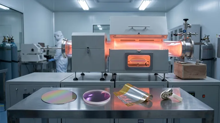
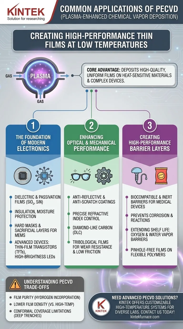
At its core, Plasma-Enhanced Chemical Vapor Deposition (PECVD) is a foundational technology for creating high-performance thin films. Its applications span a vast range of industries, most notably in semiconductor fabrication for depositing dielectric layers like silicon nitride, in optics for creating anti-reflective coatings, and for applying protective barrier layers on everything from food packaging to medical implants.
The true power of PECVD lies in its ability to deposit high-quality, uniform films at significantly lower temperatures than other methods. This single characteristic unlocks its use on heat-sensitive materials and complex, pre-fabricated devices, making it indispensable in modern manufacturing.
The Foundation of Modern Electronics
PECVD is the workhorse of the semiconductor industry. Its ability to build up layers of material without damaging the delicate circuitry already on a silicon wafer is critical.
Dielectric Films for Insulation and Passivation
In microchip fabrication, millions of components are packed into a tiny space. PECVD deposits thin, non-conductive films like silicon dioxide (SiO₂) and silicon nitride (SiN).
These films act as insulators to prevent electrical short circuits between conductive layers. They also serve as passivation layers, protecting the chip's surface from moisture and contamination.
Hard Masks and Sacrificial Layers
Building a microchip involves selectively etching away material. PECVD is used to deposit a hard mask, a durable temporary layer that protects specific areas during the etching process.
It is also used to create sacrificial layers, which are deposited and then later removed to create complex 3D structures, particularly in Micro-Electro-Mechanical Systems (MEMS).
Enabling Advanced Devices
The low-temperature nature of PECVD is crucial for creating devices built on top of other components. This includes Thin-Film Transistors (TFTs) for display screens, High-Brightness LEDs, and specialized lasers like VCSELs, where high temperatures would destroy the underlying device.
Enhancing Optical and Mechanical Performance
Beyond electronics, PECVD is a key process for manipulating how surfaces interact with light and physical force. The process allows for precise control over a film's properties.
Anti-Reflective and Anti-Scratch Coatings
For optical applications like eyeglass lenses, solar cells, and camera sensors, maximizing light transmission is essential. PECVD deposits anti-reflective coatings with a precisely controlled refractive index to minimize light loss.
By changing the precursor chemicals, the process can also create extremely hard, transparent films like diamond-like carbon (DLC) for anti-scratch coatings.
Tribological Films for Wear Resistance
In mechanical engineering, PECVD is used to apply tribological coatings on tools and components. These films provide exceptional hardness, wear resistance, and a low coefficient of friction, extending the life and efficiency of moving parts.
Creating High-Performance Barrier Layers
One of PECVD's most widespread applications is creating incredibly thin yet effective barriers to protect sensitive products.
Protecting Medical Devices
PECVD is used to coat medical implants and devices with a biocompatible and inert barrier. This protective layer prevents reactions between the implant and the body and protects the device itself from the corrosive environment of bodily fluids.
Extending Shelf Life in Food Packaging
The metallic lining inside a snack food bag is often a nanometer-thin layer of aluminum deposited using a similar process. PECVD is used on flexible polymers to create a dense, pinhole-free barrier against oxygen and water vapor, keeping the food fresh for longer.
Understanding the Trade-offs of PECVD
While incredibly versatile, PECVD is not a universal solution. Understanding its limitations is key to using it effectively.
The Challenge of Film Purity
Because the process uses chemical precursors in a plasma, atoms from those precursors (especially hydrogen) can become incorporated into the final film. This can impact the film's electrical properties and density.
Lower Film Density
Compared to high-temperature processes like Low-Pressure CVD (LPCVD), films deposited by PECVD are often less dense and have a lower structural quality. For applications requiring the absolute highest film purity and stability, a higher-temperature process may be necessary.
Conformal Coverage Limitations
While PECVD provides good coverage over surface features, it can struggle to deposit a perfectly uniform film inside very deep, narrow trenches. For these extreme high-aspect-ratio structures, a technique like Atomic Layer Deposition (ALD) is often preferred.
Making the Right Choice for Your Goal
Your application's primary constraint will determine if PECVD is the correct approach.
- If your primary focus is fabricating semiconductors or MEMS: PECVD is indispensable for depositing critical dielectric and passivation layers without damaging underlying components.
- If your primary focus is enhancing surface properties: PECVD provides precise control over film thickness, refractive index, and hardness for applications like anti-reflective coatings and wear resistance.
- If your primary focus is creating barriers on heat-sensitive materials: The low-temperature nature of PECVD makes it the ideal choice for coating polymers, plastics, and biomedical devices.
Ultimately, PECVD's versatility stems from its unique ability to engineer high-performance thin films where heat is the enemy.
Summary Table:
| Application Area | Key Uses | Materials/Properties |
|---|---|---|
| Electronics | Dielectric films, passivation, MEMS | Silicon nitride, silicon dioxide |
| Optics | Anti-reflective coatings, scratch resistance | Diamond-like carbon, precise refractive index |
| Barrier Layers | Medical implants, food packaging | Biocompatible films, oxygen/water vapor barriers |
| Mechanical | Wear-resistant coatings | Tribological films, low friction |
Need advanced PECVD solutions for your lab? KINTEK leverages exceptional R&D and in-house manufacturing to provide diverse laboratories with cutting-edge high-temperature furnace systems, including CVD/PECVD Systems. Our strong deep customization capability ensures we precisely meet your unique experimental requirements, from semiconductor fabrication to optical coatings. Contact us today to enhance your research and production efficiency!
Visual Guide
Related Products
- Slide PECVD Tube Furnace with Liquid Gasifier PECVD Machine
- RF PECVD System Radio Frequency Plasma Enhanced Chemical Vapor Deposition
- Inclined Rotary Plasma Enhanced Chemical Deposition PECVD Tube Furnace Machine
- Inclined Rotary Plasma Enhanced Chemical Deposition PECVD Tube Furnace Machine
- Multi Heating Zones CVD Tube Furnace Machine for Chemical Vapor Deposition Equipment
People Also Ask
- What are the advantages of using a tube furnace CVD system for Cu(111)/graphene? Superior Scalability and Quality
- In which industries is the tube furnace commonly used? Essential for Materials Science, Energy, and More
- What plasma source is used in PE-CVD tube furnaces? Unlock Low-Temperature, High-Quality Deposition
- How does a hydrogen reduction environment in an industrial tube furnace facilitate gold-copper alloy microspheres?
- What role does a Tube Furnace play in the CVD growth of carbon nanotubes? Achieve High-Purity CNT Synthesis


