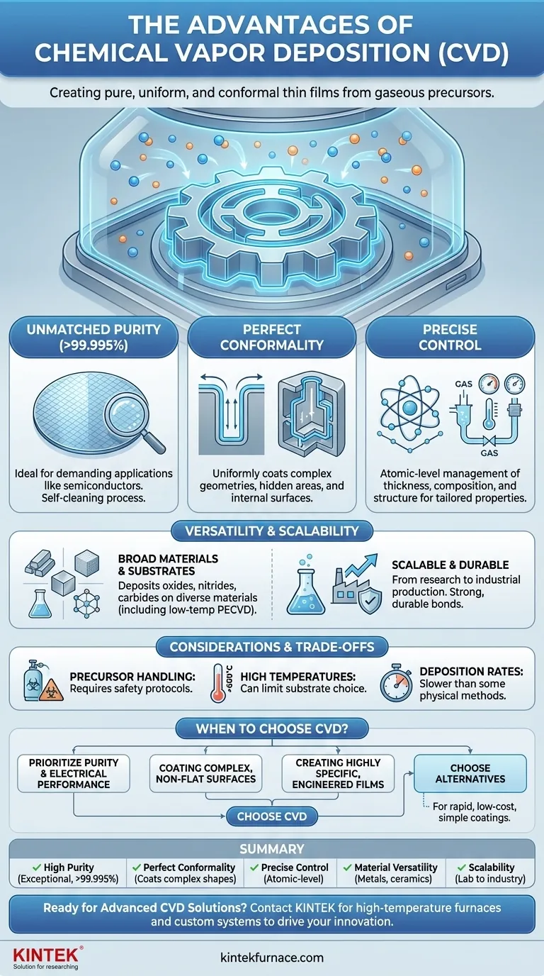
At its core, Chemical Vapor Deposition (CVD) offers the ability to create exceptionally pure, uniform, and conformal thin films on virtually any surface, no matter how complex. This process moves beyond simply coating a surface; it constructs a new material layer from gaseous precursors, providing unparalleled control over the final film’s properties and performance.
The fundamental advantage of CVD is not just what it deposits, but how. By building films from a gaseous state, it achieves a level of precision in purity, thickness, and uniformity that is often unattainable with liquid or line-of-sight deposition methods.
The Foundation of CVD: Building from the Gas Up
The defining characteristic of CVD is that the precursors—the building blocks of the film—are in a gaseous state. These gases flood a reaction chamber, ensuring they reach every exposed surface of the substrate before reacting to form the desired solid film. This "gas-up" approach is the source of its primary benefits.
Unmatched Purity for Demanding Applications
Because the process starts with highly purified precursor gases, the resulting films can achieve exceptional purity, often exceeding 99.995%.
This makes CVD indispensable in the semiconductor industry, where even minuscule impurities can ruin the performance of a microchip. The process is also inherently self-cleaning, as the reactive gases help remove contaminants.
Perfect Conformality on Complex Geometries
Unlike line-of-sight processes (like evaporation or sputtering) that struggle to coat hidden areas, the gaseous precursors in CVD can diffuse into and coat intricate shapes, deep trenches, and internal surfaces with a perfectly uniform layer.
This property, known as high conformality, is critical for applications like coating the complex internal passages of engine components, the detailed surfaces of medical implants, or the microscopic structures on a silicon wafer.
Precise Control Over Film Properties
CVD provides atomic-level control over the deposition process. By carefully managing gas flow rates, temperature, and pressure, engineers can precisely dictate the film's thickness, composition, and crystal structure.
This allows for the creation of highly customized materials engineered for specific properties, such as hardness, chemical resistance, or electrical conductivity.
Versatility and Scalability for Industry
CVD is not a niche laboratory technique; it is a robust and flexible manufacturing platform used across a wide range of industries, from aerospace to optics.
A Broad Palette of Materials
CVD is remarkably versatile and can be used to deposit a wide array of materials. This includes metals, pure alloys, and various ceramic compounds like oxides, nitrides, and carbides. This flexibility allows it to solve problems in many different fields.
Compatibility with Diverse Substrates
The process is compatible with a wide variety of base materials, including metals, ceramics, glass, and composites.
Furthermore, while traditional CVD operates at high temperatures, variants like Plasma-Enhanced CVD (PECVD) allow for low-temperature deposition. This opens the door to coating temperature-sensitive substrates, such as polymers, without damaging them.
Proven Scalability and Durability
The principles of CVD are effective at both small-scale research and large-scale industrial production. Once a process is developed, it can be reliably scaled to meet manufacturing demands.
The resulting films form a strong, durable bond with the substrate, ensuring the coating remains intact even in high-stress, high-wear, or extreme temperature environments.
Understanding the Trade-offs
No process is perfect. To make an informed decision, it's crucial to understand the practical considerations and potential downsides of CVD.
Precursor Material Handling
The precursor gases used in CVD can be toxic, flammable, or corrosive. This necessitates significant investment in safety infrastructure, handling protocols, and exhaust gas treatment systems. These materials can also be expensive, contributing to the overall cost.
High Process Temperatures
Many traditional CVD processes require high temperatures (often >600°C) to drive the chemical reactions. This can limit the choice of substrate materials to those that can withstand the heat without deforming or degrading.
Deposition Rates
In some cases, CVD can have a slower deposition rate compared to physical methods like sputtering. For applications requiring very thick coatings where ultimate purity and conformality are not the primary drivers, this can be a limitation.
Making the Right Choice for Your Goal
CVD is a powerful tool when its unique advantages align with your primary technical objective.
- If your primary focus is ultimate purity and electrical performance: CVD is the industry standard for semiconductor and electronics manufacturing for this reason.
- If your primary focus is coating a complex, non-flat, or internal surface: CVD's exceptional conformality is its most significant advantage over other methods.
- If your primary focus is creating a thin film with highly specific, engineered properties: CVD offers precise control over composition and structure that is difficult to replicate.
- If your primary focus is rapid, low-cost deposition of a simple coating: You may want to evaluate alternative methods like PVD or electroplating.
Ultimately, choosing CVD is a decision to prioritize quality, precision, and performance at the atomic level.
Summary Table:
| Advantage | Description |
|---|---|
| High Purity | Films achieve exceptional purity (>99.995%), ideal for semiconductors and sensitive applications. |
| Perfect Conformality | Gaseous precursors coat complex geometries uniformly, including internal surfaces and trenches. |
| Precise Control | Atomic-level management of thickness, composition, and structure for customized material properties. |
| Material Versatility | Deposits metals, alloys, and ceramics like oxides, nitrides, and carbides on various substrates. |
| Scalability | Effective from lab research to industrial production with durable, strong-bonded coatings. |
Ready to elevate your lab's capabilities with advanced CVD solutions? At KINTEK, we leverage exceptional R&D and in-house manufacturing to provide high-temperature furnace solutions tailored to your needs. Our product line, including CVD/PECVD Systems, Muffle, Tube, Rotary Furnaces, and Vacuum & Atmosphere Furnaces, is complemented by strong deep customization to meet your unique experimental requirements. Contact us today to discuss how our expertise can help you achieve superior thin film deposition and drive innovation in your projects!
Visual Guide
Related Products
- RF PECVD System Radio Frequency Plasma Enhanced Chemical Vapor Deposition
- 915MHz MPCVD Diamond Machine Microwave Plasma Chemical Vapor Deposition System Reactor
- MPCVD Machine System Reactor Bell-jar Resonator for Lab and Diamond Growth
- Custom Made Versatile CVD Tube Furnace Chemical Vapor Deposition CVD Equipment Machine
- HFCVD Machine System Equipment for Drawing Die Nano Diamond Coating
People Also Ask
- What are the applications of plasma enhanced chemical vapor deposition? Key Uses in Electronics, Optics & Materials
- How does film quality compare between PECVD and CVD? Choose the Best Method for Your Substrate
- What are the key advantages of PECVD technology? Achieve Low-Temperature, High-Quality Thin Film Deposition
- What is PECVD specification? A Guide to Choosing the Right System for Your Lab
- What is RF in PECVD? A Critical Control for Plasma Deposition


