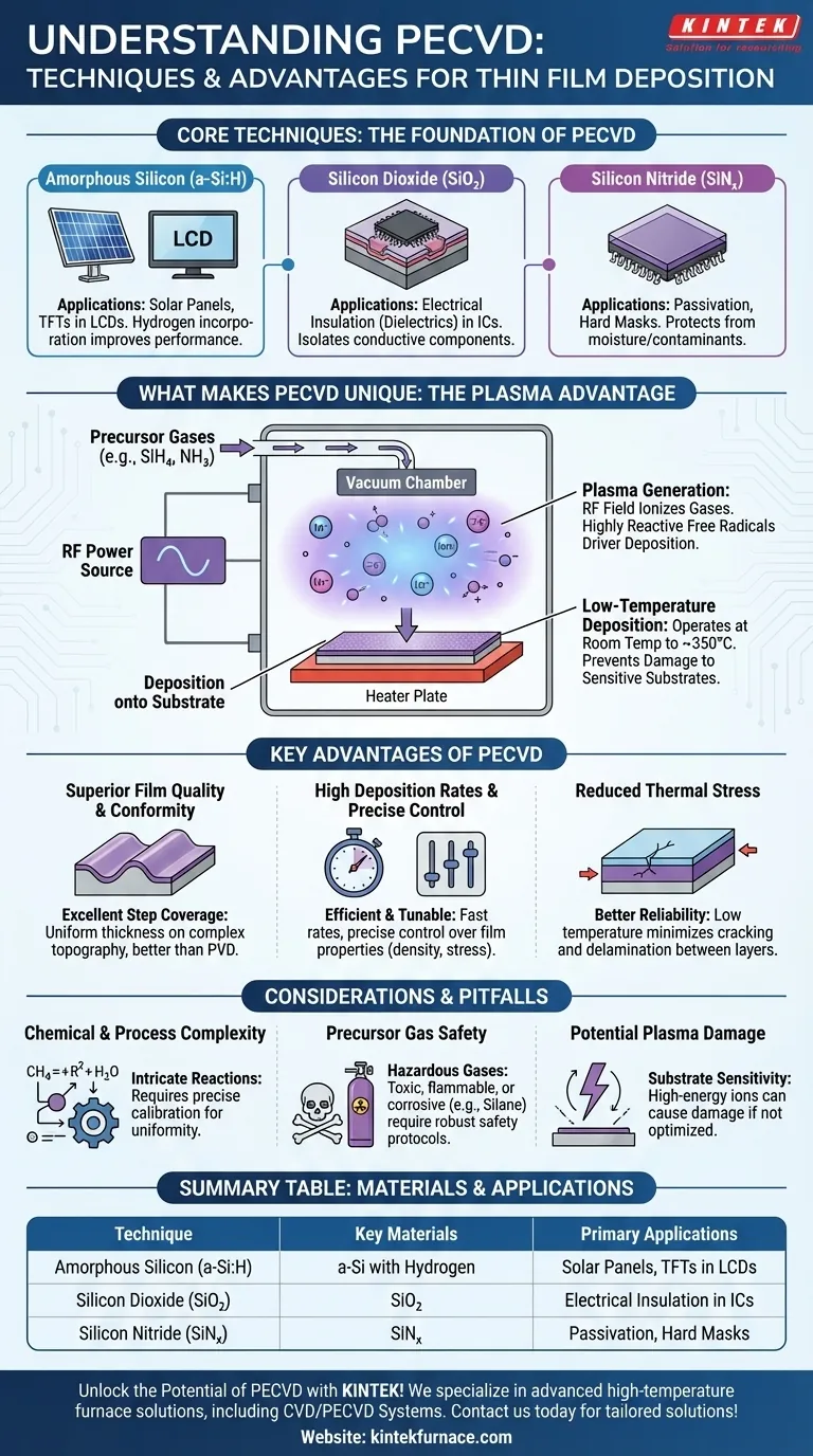
At its core, Plasma-Enhanced Chemical Vapor Deposition (PECVD) is a process that supports the deposition of several critical thin films for microfabrication. The primary techniques involve creating layers of amorphous silicon (a-Si), silicon dioxide (SiO₂), and silicon nitride (SiNₓ). These are foundational materials for manufacturing semiconductors, solar cells, and various electronic devices.
The essential value of PECVD is not just the materials it can deposit, but how it achieves the deposition. By using plasma to energize precursor gases, PECVD enables the creation of high-quality, uniform thin films at significantly lower temperatures than traditional thermal methods, making it compatible with sensitive substrates.
What Makes the PECVD Technique Unique?
Understanding PECVD requires looking beyond the resulting films and focusing on the process itself. Its distinct advantages stem from its use of plasma instead of high heat to drive the chemical reactions.
The Role of Plasma
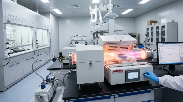
PECVD introduces precursor gases into a vacuum chamber and then uses a radio frequency (RF) electric field to ionize them, creating a glowing plasma.
This plasma contains highly reactive free radicals. These energized particles are what drive the deposition onto the substrate, rather than relying solely on thermal energy.
Low-Temperature Deposition
This is the most significant advantage of the technique. While conventional Chemical Vapor Deposition (CVD) requires very high temperatures (often >600°C), PECVD can operate anywhere from room temperature to around 350°C.
This low thermal budget prevents damage to underlying components or substrates that cannot withstand high heat, such as plastics, certain metals, or previously fabricated device layers.
Distinct System Configuration
A PECVD system is engineered specifically for this plasma process. It differs from other deposition methods like Physical Vapor Deposition (PVD) with key components.
These include a specialized RF power source to generate the plasma, precise gas distribution systems for precursor delivery, and vacuum pumps capable of maintaining the low pressures required for stable plasma.
A Closer Look at Core Deposition Techniques
The unique process of PECVD makes it ideal for depositing specific types of films that are critical in modern electronics.
Amorphous Silicon (a-Si:H) Deposition
This technique is widely used in manufacturing solar panels and the thin-film transistors (TFTs) found in LCD screens. The plasma process allows hydrogen to be incorporated into the amorphous silicon film, which "passivates" defects and improves electronic performance.
Silicon Dioxide (SiO₂) Deposition
PECVD is used to grow high-quality silicon dioxide films that serve as excellent electrical insulators (dielectrics). These layers are crucial for isolating conductive components from each other within an integrated circuit.
Silicon Nitride (SiNₓ) Deposition
Silicon nitride films are valued for their density and chemical stability. They are primarily used as a passivation layer to protect the surface of a microchip from moisture and contaminants, or as a hard mask for subsequent etching steps. The low-temperature process prevents stress and damage to the underlying device.
Understanding the Key Advantages
The low-temperature, plasma-driven nature of PECVD translates into several tangible benefits for device fabrication.
Superior Film Quality and Conformity
PECVD provides excellent step coverage, meaning it can deposit a film of uniform thickness over surfaces with complex, non-flat topography. This "conformality" is much better than line-of-sight methods like PVD.
High Deposition Rates and Control
The plasma process is highly efficient, enabling fast deposition rates which improve manufacturing throughput. Furthermore, parameters like gas flow, pressure, and RF power allow for precise control over the properties of the deposited film, such as its density, refractive index, and stress.
Reduced Thermal Stress
When layering materials with different thermal expansion coefficients, high-temperature processing can cause the films to crack or delaminate upon cooling. PECVD's low-temperature nature dramatically reduces this thermal stress, leading to better device reliability and bonding quality.
Common Pitfalls and Considerations
While powerful, the PECVD technique is not without its complexities and requires careful management to achieve optimal results.
Chemical and Process Complexity
The plasma environment involves intricate chemical reactions that can be more difficult to model and control than purely thermal processes. Achieving film uniformity and repeatable properties requires precise calibration of the system.
Precursor Gas Safety
The gases used in PECVD, such as silane (SiH₄) and ammonia (NH₃), are often toxic, flammable, or corrosive. This necessitates robust safety protocols, gas detection systems, and proper handling procedures.
Potential for Plasma-Induced Damage
Although the process is considered "gentle," the high-energy ions within the plasma can sometimes cause physical or electrical damage to extremely sensitive substrates or device layers if the process parameters are not optimized correctly.
Making the Right Choice for Your Goal
To determine if PECVD is the right technique, you must align its core strengths with your project's primary constraints.
- If your primary focus is compatibility with sensitive substrates: PECVD's low-temperature process is its most significant advantage, preventing thermal damage to polymers or pre-existing metallic layers.
- If your primary focus is creating high-quality dielectric or passivation layers: The ability to deposit dense, uniform SiO₂ and SiNₓ films for insulation and protection is a core strength of the technique.
- If your primary focus is covering complex, non-flat surfaces: PECVD offers superior conformity and step coverage compared to many line-of-sight deposition methods, ensuring complete and even coating.
Ultimately, PECVD empowers you to engineer advanced thin films in applications where the thermal budget is a critical constraint.
Summary Table:
| Technique | Key Materials | Primary Applications |
|---|---|---|
| Amorphous Silicon (a-Si:H) | a-Si with hydrogen | Solar panels, TFTs in LCDs |
| Silicon Dioxide (SiO₂) | SiO₂ | Electrical insulation in ICs |
| Silicon Nitride (SiNₓ) | SiNₓ | Passivation, hard masks |
Unlock the potential of PECVD for your lab with KINTEK! We specialize in advanced high-temperature furnace solutions, including CVD/PECVD Systems, backed by exceptional R&D and in-house manufacturing. Our deep customization capabilities ensure we can precisely meet your unique experimental needs, whether you're working with semiconductors, solar cells, or other electronic devices. Contact us today to discuss how our tailored PECVD systems can enhance your thin film deposition processes and drive innovation in your projects!
Visual Guide
Related Products
- RF PECVD System Radio Frequency Plasma Enhanced Chemical Vapor Deposition
- Slide PECVD Tube Furnace with Liquid Gasifier PECVD Machine
- Inclined Rotary Plasma Enhanced Chemical Deposition PECVD Tube Furnace Machine
- Inclined Rotary Plasma Enhanced Chemical Deposition PECVD Tube Furnace Machine
- Cylindrical Resonator MPCVD Machine System for Lab Diamond Growth
People Also Ask
- What are the key advantages of PECVD technology? Achieve Low-Temperature, High-Quality Thin Film Deposition
- What are the advantages of PECVD in film deposition? Achieve Low-Temp, High-Quality Coatings
- What is RF in PECVD? A Critical Control for Plasma Deposition
- What are the applications of plasma enhanced chemical vapor deposition? Key Uses in Electronics, Optics & Materials
- How does film quality compare between PECVD and CVD? Choose the Best Method for Your Substrate


