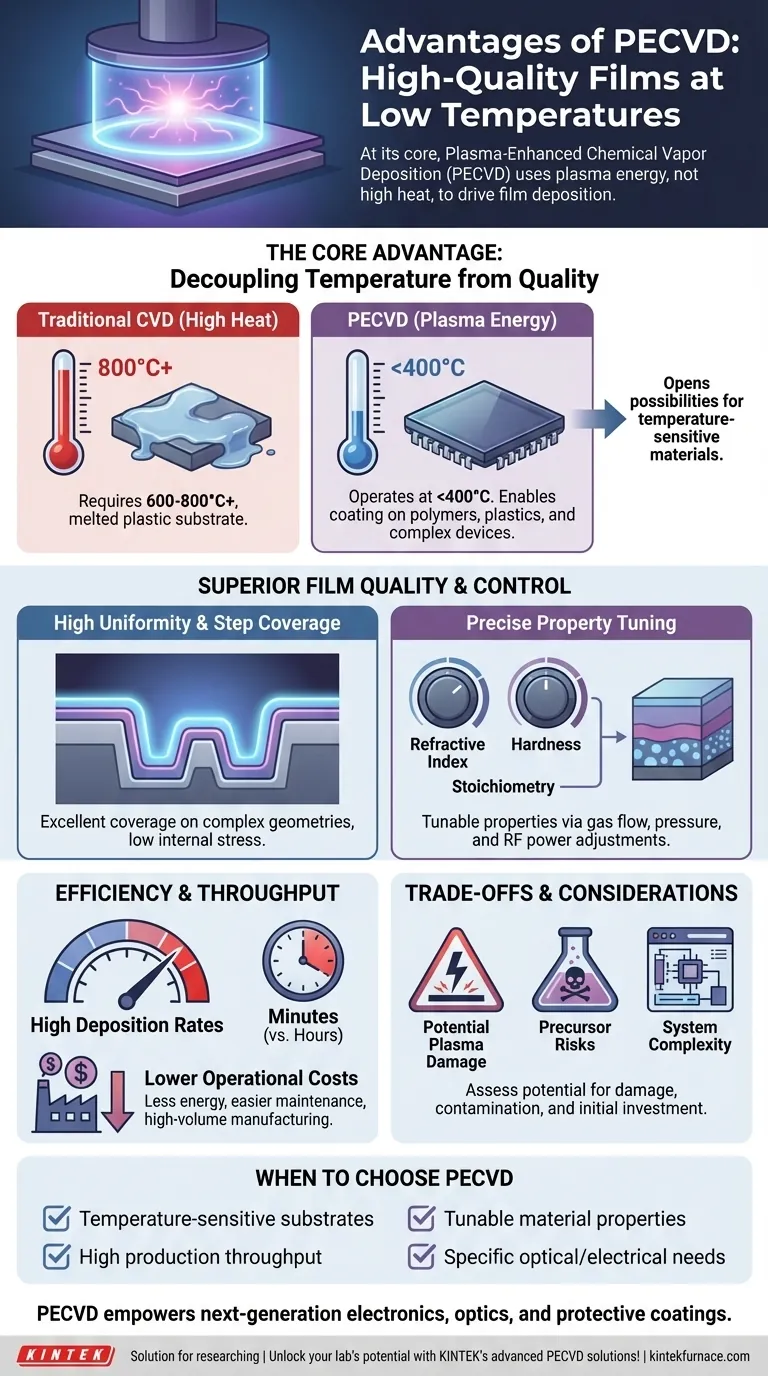
At its core, Plasma-Enhanced Chemical Vapor Deposition (PECVD) is a process that achieves high-quality film deposition without the need for extreme heat. Its primary advantages are the ability to operate at low temperatures (typically below 400°C), produce highly uniform films with excellent properties, and achieve deposition rates significantly faster than many alternative methods. This combination makes it uniquely suitable for coating temperature-sensitive materials and for high-throughput manufacturing.
The fundamental advantage of PECVD is its ability to use the energy from plasma, rather than high heat, to drive the chemical reactions needed for film deposition. This decouples film quality from the substrate's thermal budget, opening up a vast range of possibilities for advanced material engineering on sensitive substrates.
The Core Advantage: Decoupling Temperature from Quality
The most significant benefit of PECVD is its low-temperature operation, which fundamentally changes what is possible in thin-film deposition. It breaks the traditional reliance on thermal energy to create high-quality materials.
Operating at Low Temperatures
Unlike conventional Chemical Vapor Deposition (CVD) which often requires temperatures of 600-800°C or higher, PECVD typically operates around 350°C.
This lower thermal budget is critical for depositing films onto substrates that cannot withstand high heat. This includes polymers, plastics, and complex semiconductor devices that already have metallic layers or other structures that would be damaged by high temperatures.
Achieving High-Quality, Uniform Films
The plasma environment provides the energy to dissociate precursor gases and enable surface reactions, compensating for the lack of thermal energy. This results in films with exceptional characteristics.
PECVD is known for depositing films with high uniformity across the entire substrate and excellent step coverage, meaning it can evenly coat complex, non-flat geometries. The resulting films also exhibit low internal stress, making them less prone to cracking and improving adhesion to the substrate.
Gaining Precise Control Over Film Properties
The plasma process gives engineers a high degree of control over the final material. By adjusting parameters like gas flow, pressure, and RF power, it is possible to precisely tune the film's properties.
This includes controlling the stoichiometry (the exact ratio of elements in a compound), refractive index, hardness, and electrical characteristics. This level of control is essential for fabricating optical coatings, dielectrics, and protective layers with specific performance requirements.
Driving Efficiency and Throughput
Beyond its technical capabilities, PECVD provides significant economic and production advantages, making it a cost-effective solution for many industries, particularly in high-volume manufacturing.
Accelerating Deposition Rates
The plasma significantly enhances the rate of chemical reactions, allowing PECVD to achieve high deposition rates. This means films can often be deposited in minutes rather than the hours required by some traditional methods.
This speed directly translates to higher production throughput, reducing manufacturing time and cost per wafer or part.
Lowering Operational Costs
The efficiency of PECVD extends to its operational footprint. Low-temperature operation consumes less energy by eliminating the need for power-hungry furnaces.
Furthermore, many PECVD systems are designed for relatively easy chamber cleaning, which reduces equipment downtime and increases overall production efficiency.
Understanding the Trade-offs and Considerations
While powerful, PECVD is not a universal solution. An objective assessment requires understanding its potential limitations.
Potential for Plasma-Induced Damage
The high-energy ions within the plasma can, in some cases, cause damage to the surface of an extremely sensitive substrate or the film being deposited. This is a critical consideration for certain electronic or optical applications where even minimal surface damage is unacceptable.
Precursor and Contamination Risks
Like all CVD processes, PECVD relies on chemical precursors that can be hazardous or toxic. More specific to PECVD, the plasma can sometimes incorporate elements from the precursor gases (like hydrogen) into the film as impurities, which may affect its performance.
System Complexity and Cost
A PECVD system, with its vacuum chamber, gas delivery system, and RF plasma generator, is more complex than a simple thermal furnace. This can result in a higher initial capital investment and require more sophisticated maintenance and process control.
Making the Right Choice for Your Application
Selecting the right deposition technique depends entirely on your project's specific constraints and goals.
- If your primary focus is temperature-sensitive substrates: PECVD is the clear choice for depositing high-quality films on polymers, plastics, or fully fabricated devices without causing thermal damage.
- If your primary focus is high production throughput: The high deposition rates and operational efficiency of PECVD make it ideal for cost-effective, high-volume manufacturing.
- If your primary focus is tunable material properties: PECVD provides superior control for engineering films with a specific refractive index, stress level, or hardness.
- If your primary focus is absolute film purity with zero surface damage: You may need to consider alternatives like Atomic Layer Deposition (ALD) or low-pressure CVD if your substrate is extremely sensitive to plasma and requires the lowest possible impurity levels.
By enabling the creation of high-performance films without high heat, PECVD empowers the development of next-generation electronics, optics, and protective coatings.
Summary Table:
| Advantage | Description |
|---|---|
| Low-Temperature Operation | Enables deposition on heat-sensitive materials like polymers and semiconductors without damage, typically below 400°C. |
| High-Quality, Uniform Films | Provides excellent step coverage, low internal stress, and superior adhesion for consistent coatings. |
| Precise Control Over Properties | Allows tuning of stoichiometry, refractive index, hardness, and electrical characteristics via plasma parameters. |
| High Deposition Rates | Accelerates production with faster film growth, reducing manufacturing time and costs. |
| Lower Operational Costs | Reduces energy consumption and downtime through efficient, low-heat processes and easy maintenance. |
Unlock the full potential of your lab with KINTEK's advanced PECVD solutions! Leveraging exceptional R&D and in-house manufacturing, we provide diverse laboratories with high-temperature furnace systems, including CVD/PECVD Systems, designed for precision and efficiency. Our strong deep customization capability ensures we meet your unique experimental needs, delivering high-quality, uniform films for temperature-sensitive substrates and high-throughput applications. Contact us today to discuss how our tailored PECVD systems can enhance your material engineering and drive innovation in your projects!
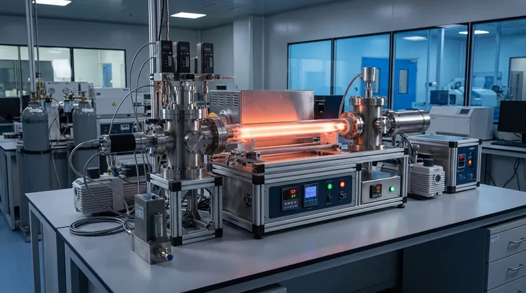
Visual Guide
Related Products
- RF PECVD System Radio Frequency Plasma Enhanced Chemical Vapor Deposition
- Slide PECVD Tube Furnace with Liquid Gasifier PECVD Machine
- Inclined Rotary Plasma Enhanced Chemical Deposition PECVD Tube Furnace Machine
- Inclined Rotary Plasma Enhanced Chemical Deposition PECVD Tube Furnace Machine
- Cylindrical Resonator MPCVD Machine System for Lab Diamond Growth
People Also Ask
- What is PECVD specification? A Guide to Choosing the Right System for Your Lab
- What is the role of RF power in PECVD and how does the RF-PECVD process work? Master Thin Film Deposition Control
- What is RF in PECVD? A Critical Control for Plasma Deposition
- How does film quality compare between PECVD and CVD? Choose the Best Method for Your Substrate
- How is silicon dioxide deposited from tetraethylorthosilicate (TEOS) in PECVD? Achieve Low-Temperature, High-Quality SiO2 Films


