At its core, Plasma-Enhanced Chemical Vapor Deposition (PECVD) controls film properties by precisely manipulating the energy and chemical composition of the plasma environment within the deposition chamber. By adjusting parameters like gas flow rates, RF power, frequency, and temperature, an operator is directly altering the chemical reactions and physical bombardment occurring at the substrate surface, which in turn dictates the final characteristics of the deposited film.
The fundamental principle of PECVD control is its ability to use plasma-generated energy—rather than high thermal energy—to drive chemical reactions. This allows for fine-tuning the deposition process at low temperatures, providing a wide array of "levers" to pull to engineer a film's specific mechanical, optical, and electrical properties.
The Core Mechanism: From Process Inputs to Film Outputs
To understand how PECVD achieves such precise control, you must understand how each process input influences the plasma and, consequently, the film itself. The process is a chain of cause and effect.
The Role of Plasma Energy
The "PE" in PECVD is the most critical element. An electric field (typically Radio Frequency, or RF) is used to energize a gas mixture into a plasma state, creating a soup of ions, electrons, and highly reactive neutral radicals.
The RF power and frequency are primary levers. Increasing the power generally increases the density of the plasma, leading to a higher concentration of reactive species and a faster deposition rate. However, it also increases ion bombardment energy, which can make a film denser but may also increase its internal stress.
Controlling Chemical Composition
The film is built atom by atom from precursor gases. The properties of the final film are directly tied to its elemental makeup (stoichiometry).
By adjusting the flow rates and ratios of different precursor gases, you can precisely control this composition. For instance, when depositing silicon oxynitride (SiON), varying the ratio of silane (SiH4), ammonia (NH3), and nitrous oxide (N2O) allows for continuous tuning of the film's refractive index and etch rate.
The Influence of Temperature and Pressure
While PECVD is a low-temperature process compared to standard CVD, substrate temperature is still a vital control parameter.
A modest increase in temperature provides surface atoms with more energy to move around (adatom mobility). This helps them find more stable lattice sites, resulting in a denser, more stable film with lower intrinsic hydrogen content.
Chamber pressure affects the mean free path of gas molecules. Lower pressures lead to fewer collisions in the gas phase and more directional deposition, while higher pressures can increase deposition rate but may compromise uniformity across the substrate.
A Breakdown of Key Control Parameters
While the principles are interconnected, it's useful to think of the main adjustable parameters as individual control knobs for the process.
Gas Flow Rates
This is the most direct way to control the film's chemical makeup. Introducing more of a specific precursor gas will increase its incorporation into the film, changing properties like conductivity, refractive index, and chemical resistance.
RF Power and Frequency
This knob primarily governs the plasma's energy and density. Higher power boosts deposition speed but can also lead to film damage or high compressive stress due to intense ion bombardment. The choice of frequency (e.g., low-frequency vs. high-frequency RF) also significantly impacts ion energy and film stress.
Substrate Temperature
Temperature influences film density, chemical bond quality, and stress. It is a critical parameter for driving off unwanted byproducts, like hydrogen, which can affect the film's long-term stability and electrical properties.
Chamber Geometry and Hardware
Less frequently adjusted but fundamentally important are aspects like the distance between the electrodes and the gas inlet configuration. These hardware factors determine the uniformity of the plasma and the flow of reactive gases across the substrate, directly impacting the film's thickness and property consistency.
Understanding the Trade-offs
Achieving a perfect film requires balancing competing factors. Understanding these trade-offs is the mark of an experienced process engineer.
Rate vs. Quality
Increasing deposition rate is often a primary goal for manufacturing throughput. However, faster deposition—achieved through higher power or pressure—often comes at the expense of film quality. This can manifest as lower density, higher impurity content (especially hydrogen), and elevated internal stress.
Stress vs. Density
Creating a dense, void-free film is crucial for applications like moisture barriers or high-quality dielectrics. Methods to increase density, such as higher ion energy, almost invariably increase the film's compressive stress. Excessive stress can cause the film to crack or delaminate from the substrate.
Uniformity vs. Simplicity
Achieving excellent film uniformity (consistent thickness and properties across an entire wafer) is a complex challenge. It requires careful tuning of gas flow dynamics, chamber pressure, and plasma distribution, often involving more sophisticated hardware and process control than a simple, centered deposition.
Making the Right Choice for Your Goal
Your optimal PECVD process settings are entirely dependent on the intended application of your thin film.
- If your primary focus is optical properties (e.g., anti-reflection coatings): Concentrate on meticulously controlling the gas flow ratios to fine-tune the film's stoichiometry and, therefore, its refractive index.
- If your primary focus is electrical insulation (e.g., gate dielectrics): Prioritize process cleanliness and moderate temperatures to create a dense, low-defect film with minimal hydrogen content to ensure low leakage current.
- If your primary focus is mechanical protection (e.g., wear-resistant layers): Employ higher RF power to increase ion bombardment, which enhances film density and hardness, but carefully monitor and manage the resulting compressive stress.
- If your primary focus is high throughput for manufacturing: Increase gas flows and RF power to maximize deposition rate, but implement in-line metrology to ensure film properties remain within an acceptable tolerance window.
Ultimately, the versatility of PECVD stems from its ability to decouple the energy source from the heat source, empowering you to engineer thin films with properties tailored to a specific purpose.
Summary Table:
| Control Parameter | Key Influence on Film Properties | Common Adjustments |
|---|---|---|
| Gas Flow Rates | Chemical composition, refractive index, conductivity | Vary precursor ratios (e.g., SiH4, NH3, N2O) |
| RF Power & Frequency | Deposition rate, density, stress | Increase power for higher density; adjust frequency for stress control |
| Substrate Temperature | Film density, hydrogen content, stability | Raise temperature for denser, more stable films |
| Chamber Pressure | Uniformity, deposition rate | Lower pressure for directional deposition; higher for faster rate |
Unlock Precision in Your Thin-Film Processes with KINTEK
Are you striving to achieve superior control over film properties like density, stress, and uniformity in your laboratory? KINTEK leverages exceptional R&D and in-house manufacturing to provide advanced high-temperature furnace solutions tailored to your needs. Our product line includes Muffle, Tube, Rotary Furnaces, Vacuum & Atmosphere Furnaces, and CVD/PECVD Systems, all backed by strong deep customization capabilities to precisely meet your unique experimental requirements. Whether you're working on optical coatings, electrical insulation, or mechanical protection, we can help you optimize your PECVD processes for better results.
Contact us today to discuss how our solutions can enhance your research and development—let's engineer the perfect thin films together!
Visual Guide

Related Products
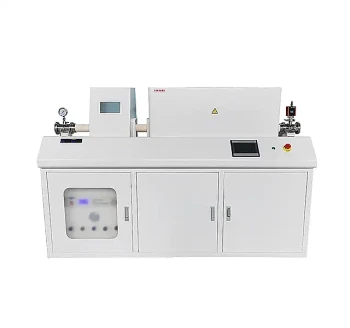
- Slide PECVD Tube Furnace with Liquid Gasifier PECVD Machine
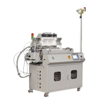
- Inclined Rotary Plasma Enhanced Chemical Deposition PECVD Tube Furnace Machine
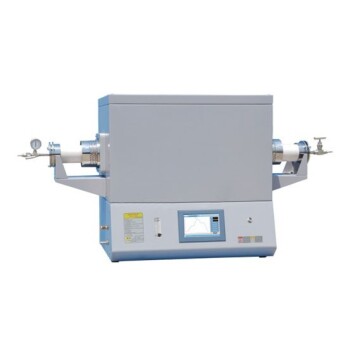
- Custom Made Versatile CVD Tube Furnace Chemical Vapor Deposition CVD Equipment Machine
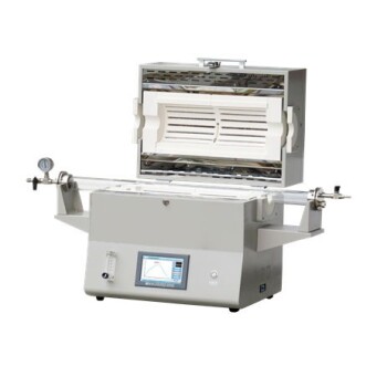
- Multi Heating Zones CVD Tube Furnace Machine for Chemical Vapor Deposition Equipment
- 1700℃ High Temperature Laboratory Tube Furnace with Alumina Tube
People Also Ask
- Why are high-purity quartz boats used for graphene oxide reduction? Ensure Chemical Purity & Thermal Stability
- How does PECVD contribute to semiconductor manufacturing? Enable Low-Temperature, High-Quality Film Deposition
- What are the classifications of CVD based on vapor characteristics? Optimize Your Thin Film Deposition Process
- How does chemical vapour deposition (CVD) differ from PVD? Key Differences in Thin-Film Coating Methods
- What are the drawbacks of CVD compared to PECVD? Key Limitations for Your Lab
