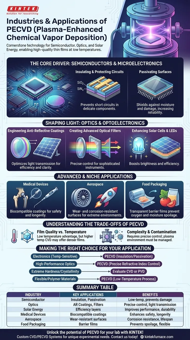
In short, Plasma-Enhanced Chemical Vapor Deposition (PECVD) is a cornerstone technology primarily used in the semiconductor, optics, and solar energy industries. Its applications also extend into critical sectors like medical devices, aerospace, and even food packaging, where it is used to deposit highly specialized thin films.
The central value of PECVD is its ability to create high-quality, functional coatings at low temperatures. This allows for the treatment of heat-sensitive materials, like complex microchips or plastics, which would be damaged or destroyed by traditional high-temperature deposition methods.
The Core Driver: Semiconductors and Microelectronics
PECVD is indispensable to the microelectronics industry because modern processors and memory chips cannot withstand high heat during manufacturing. The technology solves this problem by using plasma to energize the chemical reactions instead of heat.
### Insulating and Protecting Circuits
Transistors on a silicon wafer are incredibly small and delicate. PECVD is used to deposit thin layers of insulating materials, such as silicon dioxide (SiO₂) and silicon nitride (SiNₓ), between the metal layers of a chip.
This electrical insulation is critical for preventing short circuits. The low-temperature nature of PECVD ensures that the underlying integrated circuits are not damaged during this crucial step.
### Passivating Surfaces
Surface passivation is the process of making a material's surface less reactive. In semiconductors, PECVD deposits a final protective layer that shields the chip from moisture, chemicals, and physical damage. This dramatically increases the device's reliability and lifespan.
Shaping Light: Optics and Optoelectronics
The ability of PECVD to precisely control a film's thickness and composition makes it ideal for manufacturing optical components where every nanometer matters.
### Engineering Anti-Reflective Coatings
PECVD is used to apply multi-layer coatings to lenses, solar panels, and displays. These coatings are engineered with a specific refractive index to minimize light reflection and maximize light transmission, improving the efficiency of solar cells and the clarity of optical devices like glasses and camera lenses.
### Creating Advanced Optical Filters
By carefully tuning the deposition process, PECVD can create films that selectively block or pass specific wavelengths of light. This is essential for manufacturing sophisticated optical filters, colored lenses, and scientific instruments like photometers.
### Enhancing Solar Cells and LEDs
In photovoltaics, PECVD is a standard for depositing the anti-reflective and passivation layers that are critical for high-efficiency solar cells. For LEDs, it helps create layers that improve light extraction, making the device brighter and more efficient.
Advanced and Niche Applications
Beyond its primary uses, PECVD's versatility has been adapted for other demanding fields.
### Ensuring Biocompatibility for Medical Devices
PECVD can deposit thin, inert, and biocompatible coatings on medical implants and surgical tools. These layers create a barrier that prevents rejection by the body and improves the device's durability.
### Building Wear-Resistant Surfaces
For mechanical and aerospace applications, PECVD is used to create extremely hard and corrosion-resistant coatings. These protective films can be applied to parts operating in extreme environments to extend their operational life.
### Improving Food Packaging
In a more specialized application, PECVD is used to deposit ultra-thin glass-like layers (SiOₓ) on plastic films for food packaging. This creates a transparent, flexible barrier that prevents oxygen and moisture from spoiling the contents.
Understanding the Trade-offs of PECVD
While powerful, PECVD is not a universal solution. Its benefits come with specific limitations that are important to understand.
### Film Quality vs. Temperature
The primary advantage of PECVD is its low processing temperature. However, films deposited at higher temperatures via traditional Chemical Vapor Deposition (CVD) can sometimes be denser or have a more ordered crystalline structure, which may be required for certain niche electronic or mechanical applications.
### Complexity and Contamination
PECVD systems are complex vacuum chambers that require precise control over gas flows, pressure, and plasma power. This makes the equipment and process more expensive than simpler methods. The plasma environment can also incorporate impurities, such as hydrogen, into the film, which must be carefully managed.
Making the Right Choice for Your Application
Your choice of deposition technology depends entirely on the properties of your substrate and the desired function of the coating.
- If your primary focus is on electronics with temperature-sensitive components: PECVD is almost always the correct choice for depositing insulating and passivation layers.
- If your primary focus is on high-performance optical coatings: PECVD provides the precise control over the refractive index and thickness needed for anti-reflective layers and filters.
- If your primary focus is on extreme hardness or crystallinity: You should evaluate PECVD against higher-temperature CVD or Physical Vapor Deposition (PVD) to find the optimal balance for your needs.
- If your primary focus is on coating flexible or polymer-based materials: PECVD's low-temperature process makes it one of the few viable technologies for the job.
Ultimately, understanding where PECVD excels allows you to leverage its unique low-temperature capabilities to solve specific and challenging material science problems.
Summary Table:
| Industry | Key Applications | Benefits |
|---|---|---|
| Semiconductor | Insulation, passivation | Low-temperature processing, prevents circuit damage |
| Optics | Anti-reflective coatings, filters | Precise thickness control, enhanced light transmission |
| Solar Energy | Efficiency layers for cells | Improves performance, durability |
| Medical Devices | Biocompatible coatings | Enhances safety, longevity |
| Aerospace | Wear-resistant surfaces | Corrosion resistance, extended lifespan |
| Food Packaging | Barrier films | Prevents spoilage, flexible application |
Unlock the potential of PECVD for your lab with KINTEK! We specialize in advanced high-temperature furnace solutions, including our versatile CVD/PECVD Systems, backed by exceptional R&D and in-house manufacturing. Our deep customization capabilities ensure we meet your unique experimental needs, whether you're in semiconductors, optics, or other industries requiring precise thin film deposition. Contact us today to discuss how we can enhance your research and production efficiency with tailored solutions!
Visual Guide
Related Products
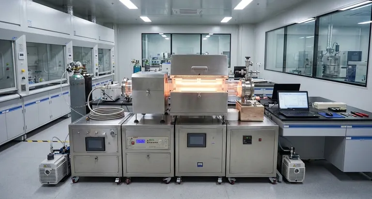
- Slide PECVD Tube Furnace with Liquid Gasifier PECVD Machine
- RF PECVD System Radio Frequency Plasma Enhanced Chemical Vapor Deposition
- Inclined Rotary Plasma Enhanced Chemical Deposition PECVD Tube Furnace Machine
- Inclined Rotary Plasma Enhanced Chemical Deposition PECVD Tube Furnace Machine
- Multi Heating Zones CVD Tube Furnace Machine for Chemical Vapor Deposition Equipment
People Also Ask
- In which industries is the tube furnace commonly used? Essential for Materials Science, Energy, and More
- How does a hydrogen reduction environment in an industrial tube furnace facilitate gold-copper alloy microspheres?
- How does PECVD equipment contribute to TOPCon bottom cells? Mastering Hydrogenation for Maximum Solar Efficiency
- What is plasma in the context of PECVD? Unlock Low-Temperature Thin Film Deposition
- What plasma source is used in PE-CVD tube furnaces? Unlock Low-Temperature, High-Quality Deposition


