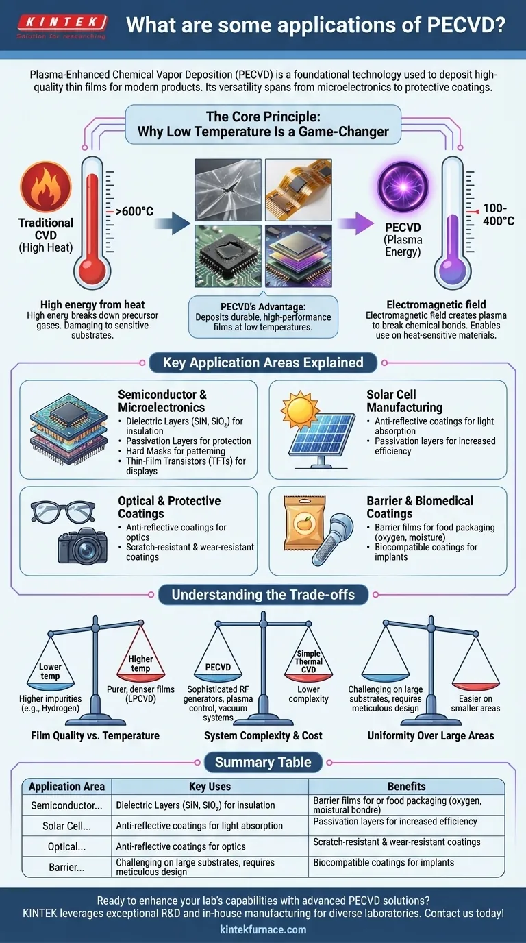
At its core, Plasma-Enhanced Chemical Vapor Deposition (PECVD) is a foundational technology used to deposit high-quality thin films for a vast array of modern products. Its applications span from the microelectronics in your smartphone and the solar panels on a roof to protective coatings on medical implants and food packaging. PECVD's versatility makes it a cornerstone of advanced manufacturing and material science.
The critical advantage of PECVD is its ability to deposit durable, high-performance films at low temperatures. This single characteristic unlocks its use on heat-sensitive materials like polymers and complex semiconductor devices, which would be damaged or destroyed by traditional high-temperature deposition methods.
The Core Principle: Why Low Temperature Is a Game-Changer
To understand PECVD's applications, you must first grasp its fundamental benefit over other methods. The goal is always to deposit a solid thin film from a gas precursor.
The Problem with High-Temperature Deposition
Traditional Chemical Vapor Deposition (CVD) relies on extreme heat (often >600°C) to provide the energy needed to break down precursor gases and initiate the chemical reaction that forms the film on a substrate.
This works well for robust materials like bare silicon wafers but is completely unsuitable for substrates that cannot withstand high temperatures, such as plastics, flexible electronics, or multi-layered semiconductor chips where heat could ruin previously fabricated components.
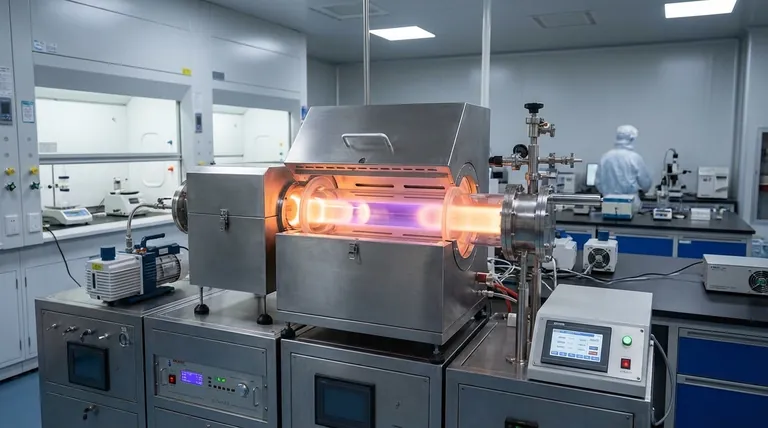
PECVD's Solution: Energy from Plasma, Not Heat
PECVD circumvents the need for high thermal energy by using an electromagnetic field (typically radio frequency) to excite the precursor gases into a plasma.
This plasma—a highly energetic state of matter—provides the energy required to break chemical bonds and drive the deposition reaction. Because the energy comes from the plasma and not thermal heating of the substrate, the process can run at much lower temperatures, often in the 100-400°C range.
Key Application Areas Explained
This low-temperature capability is the direct reason why PECVD is indispensable across several key industries.
Semiconductor and Microelectronics Fabrication
This is PECVD's most significant application. It is used to build the complex, multi-layered structures of integrated circuits (ICs), LEDs, and micro-electromechanical systems (MEMS).
Key uses include:
- Dielectric Layers: Depositing films like silicon nitride (SiN) and silicon dioxide (SiO₂) to electrically isolate conductive layers from one another.
- Passivation Layers: Applying a final protective film (often SiN) over a finished microchip to shield it from moisture, contamination, and physical damage.
- Hard Masks: Creating durable layers that define patterns for subsequent etching steps in the fabrication process.
- Thin-Film Transistors (TFTs): Essential for manufacturing modern displays, where films must be deposited on large glass panels that cannot tolerate high heat.
Solar Cell Manufacturing
Efficiency in solar cells (photovoltaics) depends on manipulating light and charge carriers with precisely engineered thin films.
PECVD is critical for depositing anti-reflective coatings that maximize light absorption and for creating passivation layers that prevent energy loss at the silicon surface, directly increasing the cell's power output.
Optical and Protective Coatings
The process allows for precise control over a film's density, composition, and thickness, which in turn controls its optical properties like refractive index.
This makes it ideal for depositing anti-reflective coatings on eyeglass lenses, camera optics, and solar panels. It is also used to create hard, scratch-resistant coatings and wear-resistant tribological coatings for mechanical components.
Barrier and Biomedical Coatings
PECVD can produce extremely dense and inert films that act as powerful barriers.
In food packaging, a microscopically thin PECVD layer on a polymer film (like in a chip bag) prevents oxygen and moisture from spoiling the contents. For medical devices, these same inert properties are used to create biocompatible coatings on implants, improving their durability and preventing adverse reactions with the body.
Understanding the Trade-offs
While powerful, PECVD is not a universal solution. Understanding its limitations is crucial for making informed engineering decisions.
Film Quality vs. Temperature
The primary trade-off is film purity. Because PECVD operates at lower temperatures, the deposited films often contain a higher concentration of impurities, most notably hydrogen, from the precursor gases.
While perfectly acceptable for most applications, this can impact electrical performance in some highly sensitive devices. High-temperature methods like Low-Pressure CVD (LPCVD) typically produce purer, denser films but lack the substrate versatility.
System Complexity and Cost
A PECVD system is more complex than a simple thermal CVD reactor. It requires sophisticated RF power generators, matching networks to control the plasma, and vacuum systems, which can increase capital and maintenance costs.
Uniformity Over Large Areas
Achieving a perfectly uniform plasma and, consequently, a perfectly uniform film thickness over very large substrates can be challenging. It requires meticulous reactor design and process control to ensure consistent results, especially in mass production.
Making the Right Choice for Your Goal
The decision to use PECVD is driven by the requirements of your substrate and the desired film properties.
- If your primary focus is electrical insulation on semiconductor devices: PECVD is the industry standard for depositing high-quality silicon dioxide and silicon nitride on temperature-sensitive wafers.
- If your primary focus is protecting a finished product: The dense, inert passivation and barrier films from PECVD are ideal for electronics, food packaging, and medical implants.
- If your primary focus is enhancing optical performance: PECVD offers precise control over refractive index, making it perfect for creating anti-reflective and scratch-resistant coatings.
- If your primary focus is maximum film purity and density at any cost: Consider higher-temperature processes like LPCVD, but only if your substrate can survive the heat.
Ultimately, understanding PECVD's low-temperature advantage empowers you to engineer advanced materials and devices that would otherwise be impossible to create.
Summary Table:
| Application Area | Key Uses | Benefits |
|---|---|---|
| Semiconductor & Microelectronics | Dielectric layers, passivation, hard masks, TFTs | Low-temperature processing, electrical insulation, protection |
| Solar Cell Manufacturing | Anti-reflective coatings, passivation layers | Increased efficiency, light absorption |
| Optical & Protective Coatings | Anti-reflective, scratch-resistant coatings | Precise optical control, durability |
| Barrier & Biomedical Coatings | Food packaging, biocompatible implants | Barrier properties, biocompatibility |
Ready to enhance your lab's capabilities with advanced PECVD solutions?
At KINTEK, we leverage exceptional R&D and in-house manufacturing to provide diverse laboratories with cutting-edge high-temperature furnace solutions. Our product line includes Muffle, Tube, Rotary Furnaces, Vacuum & Atmosphere Furnaces, and CVD/PECVD Systems, all supported by strong deep customization capabilities to precisely meet your unique experimental requirements.
Whether you're working on semiconductors, solar cells, or protective coatings, our expertise ensures optimal performance and efficiency. Don't let substrate limitations hold you back—contact us today to discuss how we can tailor a solution for your specific needs and drive your innovations forward!
Visual Guide
Related Products
- Slide PECVD Tube Furnace with Liquid Gasifier PECVD Machine
- RF PECVD System Radio Frequency Plasma Enhanced Chemical Vapor Deposition
- Inclined Rotary Plasma Enhanced Chemical Deposition PECVD Tube Furnace Machine
- Inclined Rotary Plasma Enhanced Chemical Deposition PECVD Tube Furnace Machine
- Multi Heating Zones CVD Tube Furnace Machine for Chemical Vapor Deposition Equipment
People Also Ask
- What are the typical conditions for plasma-enhanced CVD processes? Achieve Low-Temperature Thin Film Deposition
- What are the disadvantages of tube furnace cracking when processing heavy raw materials? Avoid Costly Downtime and Inefficiency
- How does PECVD equipment contribute to TOPCon bottom cells? Mastering Hydrogenation for Maximum Solar Efficiency
- In which industries is the tube furnace commonly used? Essential for Materials Science, Energy, and More
- What are the main advantages of PECVD tube furnaces compared to CVD tube furnaces? Lower Temp, Faster Deposition, and More


