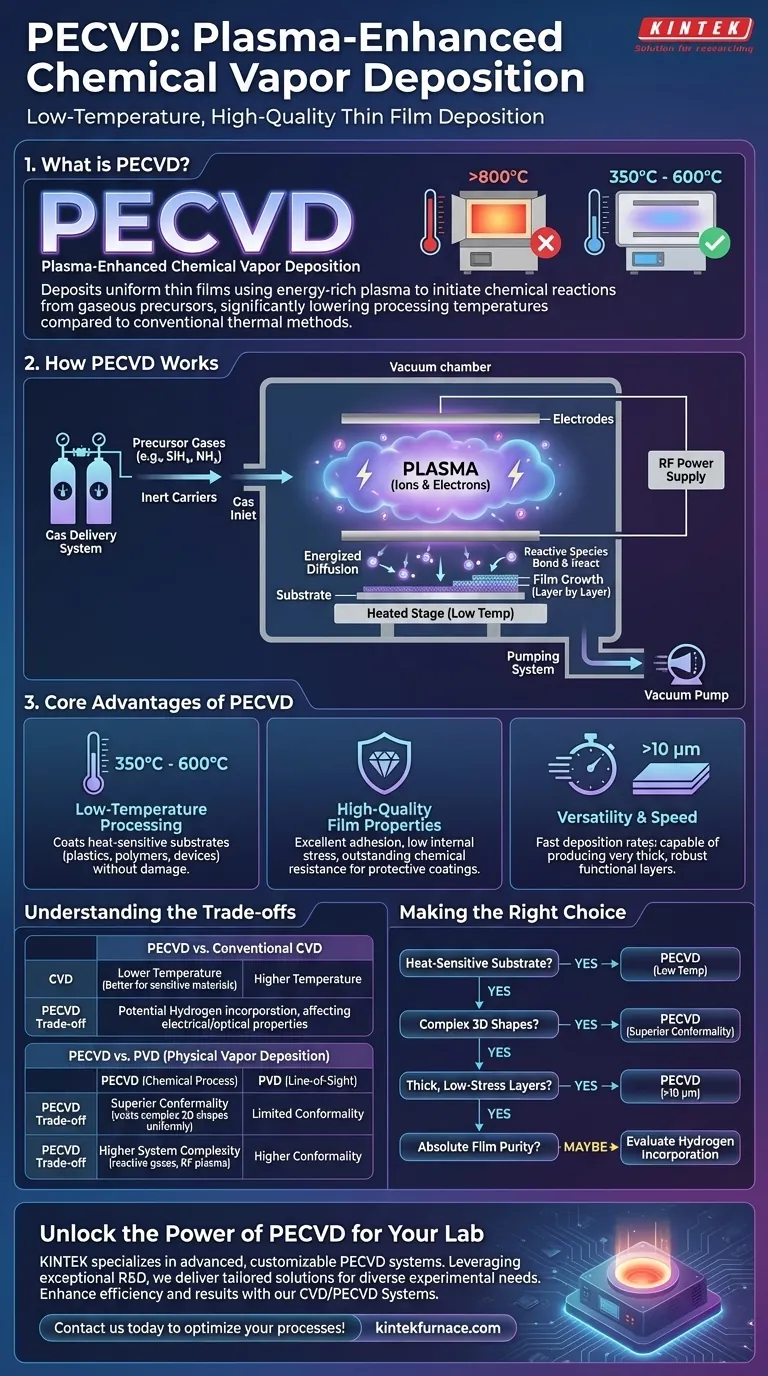
At its core, PECVD stands for Plasma-Enhanced Chemical Vapor Deposition. It is a process used to deposit high-quality, uniform thin films onto a substrate by using an energy-rich plasma to initiate a chemical reaction from gaseous precursors. Unlike conventional methods that rely solely on high heat, PECVD uses this plasma to drive the reaction, allowing for significantly lower processing temperatures.
The fundamental advantage of PECVD is its ability to overcome the high-temperature barrier of traditional deposition. By using a plasma to provide the necessary energy, it enables the growth of high-performance thin films on materials that cannot withstand extreme heat.
How PECVD Works: From Gas to Solid Film
To understand PECVD's value, you must first understand its mechanism. It is a sophisticated process that transforms specific gases into a solid, functional layer on a substrate's surface within a vacuum.
The Role of Plasma
The "Plasma-Enhanced" part of the name is the critical element. A plasma is an ionized gas—a state of matter where electrons have been stripped from their atoms, creating a mix of charged ions and free electrons.
In a PECVD system, a radio frequency (RF) power supply applies an electric field to a low-pressure gas. This energizes the free electrons, which then collide with neutral gas molecules, ionizing them and creating the plasma. This plasma serves as the energy source for the entire chemical reaction.
The Deposition Process
The process occurs in a series of controlled steps inside a vacuum chamber:
- Precursor Introduction: Precursor gases, such as silane (SiH₄) and ammonia (NH₃), are introduced into the chamber along with inert carrier gases.
- Plasma Generation: An electrical discharge between two electrodes creates the plasma, breaking down the precursor gas molecules into highly reactive ions and radicals.
- Surface Diffusion: These energized species diffuse through the vacuum and arrive at the substrate, which is typically heated but to a much lower temperature than in conventional CVD.
- Film Growth: The reactive species bond to the substrate's surface, undergoing a chemical reaction that builds up the desired thin film layer by layer.
Key System Components
A typical PECVD system is built around several core components: a vacuum chamber to control the environment, a gas delivery system with mass flow controllers for precise gas mixing, a pumping system to maintain low pressure, and an RF power source with electrodes to generate the plasma.
Why Choose PECVD? The Core Advantages
Engineers and researchers choose PECVD when other deposition methods fall short, particularly in balancing process conditions with material limitations.
Low-Temperature Processing
This is the defining advantage of PECVD. While traditional CVD can require temperatures exceeding 800°C, PECVD operates at much lower temperatures, often in the 350°C to 600°C range, and sometimes even lower. This makes it possible to coat temperature-sensitive substrates like plastics, polymers, and certain semiconductor devices without causing damage.
High-Quality Film Properties
The films deposited via PECVD exhibit desirable characteristics. They can be engineered for outstanding chemical resistance, low internal stress, and excellent adhesion. This makes them ideal for protective coatings, such as the anti-scratch layers found in high-performance optics.
Versatility and Speed
PECVD systems are known for relatively fast deposition rates. Critically, they can also produce very thick coatings—often greater than 10 micrometers—which is a significant limitation for many other deposition techniques. This capability is essential for creating robust functional or protective layers.
Understanding the Trade-offs
While powerful, PECVD is not a universal solution. Acknowledging its context and trade-offs is key to making an informed decision.
Comparison with Conventional CVD
The primary trade-off with conventional CVD is temperature versus film composition. The plasma in PECVD can cause precursor gas fragments (like hydrogen from silane) to become incorporated into the growing film. While not always detrimental, this can alter the film's electrical or optical properties, a factor that must be considered for highly sensitive applications.
Comparison with PVD (Physical Vapor Deposition)
PVD is a "line-of-sight" physical process (like sputtering), whereas PECVD is a chemical one. Because PECVD relies on a gas diffusing to the surface, it offers superior conformality, meaning it can coat complex, three-dimensional shapes more uniformly than PVD. The resulting films from PECVD are also chemically distinct, often described as more "polymer-like."
System Complexity
The use of reactive gases and RF plasma generation makes PECVD systems inherently more complex than some simpler PVD setups. This can translate to higher maintenance requirements, particularly regarding chamber cleaning to remove chemical byproducts from the deposition process.
Making the Right Choice for Your Application
Selecting the correct deposition technology hinges entirely on your end goal. Use these points as a guide.
- If your primary focus is depositing on heat-sensitive substrates: PECVD is the clear choice due to its significantly lower process temperatures.
- If your primary focus is achieving highly conformal coatings on complex 3D shapes: PECVD offers superior, uniform coverage compared to line-of-sight PVD methods.
- If your primary focus is creating thick, low-stress protective layers: PECVD excels at depositing thick ( >10 μm) films with low internal stress, ideal for mechanical or chemical barriers.
- If your primary focus is absolute film purity for high-end electronics: You must evaluate if potential hydrogen incorporation from PECVD is acceptable or if a higher-temperature, plasma-free CVD method is necessary.
By understanding these core principles, you can confidently determine if PECVD is the right tool to achieve your specific material deposition goals.
Summary Table:
| Aspect | Details |
|---|---|
| Full Name | Plasma-Enhanced Chemical Vapor Deposition |
| Primary Function | Deposits uniform thin films using plasma for low-temperature processing |
| Key Advantages | Low-temperature operation (350°C-600°C), high conformality, fast deposition, thick coatings (>10 μm) |
| Common Applications | Coatings on heat-sensitive materials, protective layers, semiconductor devices |
| Comparison | Superior to PVD for conformal coatings; lower temp than conventional CVD |
Unlock the Power of PECVD for Your Lab
Struggling with high-temperature limitations or need uniform coatings on complex shapes? KINTEK specializes in advanced high-temperature furnace solutions, including our customizable PECVD systems. Leveraging exceptional R&D and in-house manufacturing, we deliver tailored solutions for diverse laboratories, ensuring precise performance for your unique experimental needs. Our product line—featuring Muffle, Tube, Rotary Furnaces, Vacuum & Atmosphere Furnaces, and CVD/PECVD Systems—is designed to enhance efficiency and results. Don't let deposition challenges hold you back—contact us today to discuss how we can optimize your processes!
Visual Guide
Related Products
- Slide PECVD Tube Furnace with Liquid Gasifier PECVD Machine
- RF PECVD System Radio Frequency Plasma Enhanced Chemical Vapor Deposition
- Inclined Rotary Plasma Enhanced Chemical Deposition PECVD Tube Furnace Machine
- Inclined Rotary Plasma Enhanced Chemical Deposition PECVD Tube Furnace Machine
- Multi Heating Zones CVD Tube Furnace Machine for Chemical Vapor Deposition Equipment
People Also Ask
- In which industries is the tube furnace commonly used? Essential for Materials Science, Energy, and More
- What is plasma in the context of PECVD? Unlock Low-Temperature Thin Film Deposition
- What plasma source is used in PE-CVD tube furnaces? Unlock Low-Temperature, High-Quality Deposition
- What are the advantages of using a tube furnace CVD system for Cu(111)/graphene? Superior Scalability and Quality
- How does a hydrogen reduction environment in an industrial tube furnace facilitate gold-copper alloy microspheres?


