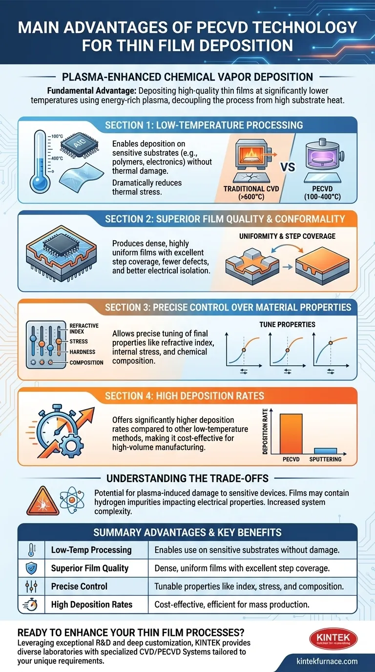
The fundamental advantage of Plasma-Enhanced Chemical Vapor Deposition (PECVD) is its ability to deposit high-quality thin films at significantly lower temperatures than traditional Chemical Vapor Deposition (CVD). This is achieved by using an energy-rich plasma to drive the necessary chemical reactions, rather than relying solely on high heat. This single innovation unlocks superior film quality, precise material property control, and compatibility with delicate electronic components.
PECVD's core innovation is its use of plasma to provide the energy for film-forming reactions, decoupling the process from high substrate temperatures. This allows for the creation of high-quality, uniform, and precisely tailored films on materials that would be damaged or destroyed by conventional high-heat methods.
The Core Mechanism: How PECVD Works
Traditional CVD requires high temperatures (often >600°C) to provide enough thermal energy to break apart precursor gases and deposit a film. PECVD circumvents this limitation by creating a plasma, a highly energetic state of matter, within the deposition chamber.
Decoupling Energy from Heat
In a PECVD system, an electric field is applied to a low-pressure gas, causing it to ionize and form a plasma.
This plasma is a mixture of ions, electrons, and highly reactive neutral species. While the electrons are extremely energetic, the ions and neutral gas atoms remain relatively cool.
The Role of Energetic Electrons
The high-energy electrons in the plasma collide with the precursor gas molecules. These collisions provide the energy needed to break chemical bonds and create reactive species that can then deposit onto the substrate surface.
Because the energy for the reaction comes from the plasma and not the substrate's heat, the substrate itself can be kept at a much lower temperature, typically between 100°C and 400°C.
Key Advantages Explained
This low-temperature, plasma-driven mechanism provides several distinct advantages that make PECVD indispensable in modern manufacturing.
Low-Temperature Processing
The ability to deposit films at low temperatures is PECVD's most transformative benefit. It enables deposition on fully fabricated devices with metal layers, polymers, or other temperature-sensitive structures without causing damage.
This is critical for adding final passivation layers to integrated circuits or fabricating devices on flexible plastic substrates. It also dramatically reduces thermal stress between film layers with different expansion coefficients.
Superior Film Quality and Conformality
PECVD produces films that are dense, highly uniform across large substrates, and have fewer pinhole defects than other low-temperature techniques.
It also provides excellent step coverage, meaning the film deposits uniformly over the complex, three-dimensional topography of a microchip. This ensures complete coverage and electrical isolation, preventing device failure.
Precise Control Over Material Properties
By adjusting parameters like gas flow, pressure, power, and frequency, operators can precisely tune the final properties of the deposited film.
This includes critical characteristics like refractive index (for optical coatings), internal stress (for mechanical stability), hardness, and chemical composition (stoichiometry). This level of control is difficult to achieve with purely thermal processes.
High Deposition Rates
Compared to other low-temperature deposition methods like sputtering, PECVD generally offers significantly higher deposition rates.
This high throughput makes it a highly cost-effective and efficient choice for high-volume manufacturing environments, directly impacting production speed and cost per unit.
Understanding the Trade-offs
While powerful, PECVD is not a universal solution. Understanding its limitations is key to using it effectively.
Potential for Plasma-Induced Damage
The same energetic plasma that enables low-temperature deposition can sometimes cause damage to sensitive electronic devices on the substrate surface. This requires careful tuning of the process to minimize ion bombardment.
Chemical Impurities
PECVD films, particularly silicon nitride and oxide, often contain significant amounts of hydrogen. The hydrogen comes from the precursor gases (like silane, SiH₄) and can become incorporated into the film.
While sometimes beneficial for passivating defects, this hydrogen can impact a film's electrical properties and thermal stability, making it unsuitable for certain high-purity applications where a high-temperature thermal process would be superior.
System and Process Complexity
A PECVD system is more complex and expensive than a simple thermal CVD furnace. The process itself has more variables to control (RF power, frequency, etc.), requiring more sophisticated process development and control.
Making the Right Choice for Your Application
Selecting the right deposition method depends entirely on the specific requirements of your film and substrate.
- If your primary focus is fabricating on temperature-sensitive substrates (like CMOS wafers or polymers): PECVD is the definitive choice for depositing high-quality dielectric films without causing thermal damage.
- If your primary focus is tuning specific optical or mechanical properties: PECVD's extensive control over parameters like refractive index and film stress gives you unparalleled flexibility.
- If your primary focus is manufacturing throughput for insulators: The high deposition rates of PECVD make it an economically sound choice for mass production.
- If your primary focus is achieving the highest possible film purity and density: A high-temperature thermal process (like LPCVD) may be a better option, as it avoids plasma-related impurities and damage.
Ultimately, understanding these core principles empowers you to select the precise tool needed to achieve your technical goals.
Summary Table:
| Advantage | Key Benefit |
|---|---|
| Low-Temperature Processing | Enables deposition on sensitive substrates (e.g., polymers, electronics) without thermal damage |
| Superior Film Quality | Produces dense, uniform films with excellent step coverage and fewer defects |
| Precise Control | Allows tuning of properties like refractive index, stress, and composition |
| High Deposition Rates | Offers cost-effective, efficient throughput for mass production |
Ready to enhance your thin film processes with advanced PECVD solutions? Leveraging exceptional R&D and in-house manufacturing, KINTEK provides diverse laboratories with high-temperature furnace solutions, including our specialized CVD/PECVD Systems. Our strong deep customization capability ensures we precisely meet your unique experimental requirements for superior film deposition. Contact us today to discuss how our tailored PECVD technologies can drive your innovations forward!
Visual Guide
Related Products
- RF PECVD System Radio Frequency Plasma Enhanced Chemical Vapor Deposition
- Slide PECVD Tube Furnace with Liquid Gasifier PECVD Machine
- Inclined Rotary Plasma Enhanced Chemical Deposition PECVD Tube Furnace Machine
- Inclined Rotary Plasma Enhanced Chemical Deposition PECVD Tube Furnace Machine
- Cylindrical Resonator MPCVD Machine System for Lab Diamond Growth
People Also Ask
- What are the advantages of PECVD in film deposition? Achieve Low-Temp, High-Quality Coatings
- What is RF in PECVD? A Critical Control for Plasma Deposition
- What are the key advantages of PECVD technology? Achieve Low-Temperature, High-Quality Thin Film Deposition
- How does film quality compare between PECVD and CVD? Choose the Best Method for Your Substrate
- What are the applications of plasma enhanced chemical vapor deposition? Key Uses in Electronics, Optics & Materials


