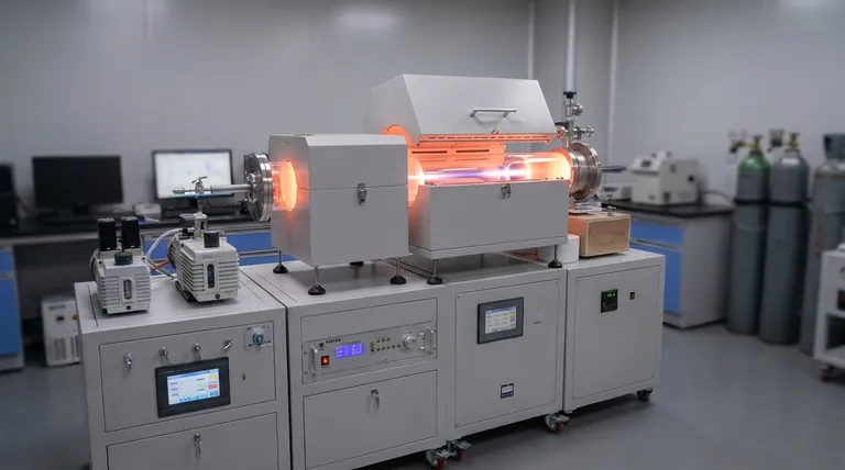
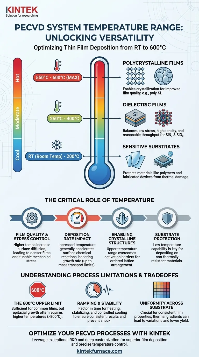
The variable temperature stage on the PECVD system operates from room temperature (RT) up to a maximum of 600 degrees Celsius. This range is designed to accommodate a wide variety of deposition processes, from those requiring minimal thermal input to those needing significant heat to achieve specific film properties.
The system's temperature range from RT to 600°C is a critical design feature. It provides the flexibility to deposit films on thermally sensitive substrates at the low end and grow higher-quality, crystalline films at the high end, making it a highly versatile tool.
The Role of Temperature in PECVD Processes
Substrate temperature is one of the most critical parameters in a Plasma-Enhanced Chemical Vapor Deposition (PECVD) process. It directly influences the energy available to precursor molecules on the substrate surface, which in turn dictates the final characteristics of the deposited film.
Controlling Film Quality and Stress
Temperature profoundly affects film density, stoichiometry, and internal stress. Higher deposition temperatures generally provide more energy for surface diffusion, allowing atoms to settle into more stable, lower-energy sites.
This typically results in denser films with lower hydrogen content (in the case of silicon nitride or amorphous silicon) and can help tune the film's mechanical stress from tensile to compressive.
Impacting Deposition Rate
The rate of film growth is strongly tied to temperature-dependent chemical reactions on the substrate surface. In many regimes, increasing the temperature will increase the deposition rate by accelerating these surface reactions.
However, at a certain point, the process can become limited by the mass transport of reactants to the surface, and further temperature increases may yield diminishing returns.
Enabling Crystalline Structures
The upper end of the temperature range is essential for depositing polycrystalline films. Temperatures approaching 600°C provide sufficient thermal energy to overcome the activation barrier for nucleation and allow atoms to arrange themselves into an ordered, crystalline lattice, such as in the case of polysilicon (poly-Si).
Protecting Sensitive Substrates
Conversely, the ability to deposit at or near room temperature is a key advantage of PECVD. This allows for the deposition of films onto substrates that cannot withstand high temperatures, such as plastics, polymers, or fully fabricated semiconductor devices with sensitive metallization layers.
Understanding the Process Limitations
While the RT to 600°C range is versatile, it's important to understand the context and trade-offs associated with it.
The 600°C Upper Limit
The 600°C maximum is sufficient for many common films, including amorphous and polycrystalline silicon, silicon dioxide, and silicon nitride. However, it is generally not high enough for depositing high-quality, single-crystal epitaxial films, which often require temperatures well above 800°C and different techniques like LPCVD or MBE.
Temperature Ramping and Stability
Achieving the setpoint temperature, especially at the higher end, is not instantaneous. The time required for the stage to ramp up and stabilize must be factored into your process recipe to ensure consistent and repeatable results. Likewise, controlled cooling is important to prevent thermal shock that can crack substrates or delaminate films.
Uniformity Across the Substrate
Maintaining a uniform temperature across the entire substrate is crucial for achieving uniform film thickness and properties. Any thermal gradients across the wafer can lead to variations in stress, composition, and deposition rate, impacting device yield.
Matching the Temperature to Your Deposition Goal
The ideal temperature is entirely dependent on your material and application. Use the following as a general guide.
- If your primary focus is depositing on sensitive substrates (like polymers): Use the low end of the range (RT to 200°C) to prevent damage to your underlying material.
- If your primary focus is high-quality dielectric films (like SiNₓ or SiO₂): Use the mid-range (250°C to 400°C) to achieve a good balance of low stress, high density, and reasonable throughput.
- If your primary focus is growing polycrystalline films (like poly-Si): Use the upper end of the range (550°C to 600°C) to provide the necessary thermal energy for crystallization.
Ultimately, this temperature range provides the flexibility to tailor deposition conditions precisely to your material and device requirements.
Summary Table:
| Temperature Range | Key Applications | Benefits |
|---|---|---|
| RT to 200°C | Sensitive substrates (e.g., polymers) | Protects materials from thermal damage |
| 250°C to 400°C | Dielectric films (e.g., SiNₓ, SiO₂) | Balances low stress, high density, and throughput |
| 550°C to 600°C | Polycrystalline films (e.g., poly-Si) | Enables crystallization and improved film quality |
Optimize your PECVD processes with KINTEK's advanced solutions! Leveraging exceptional R&D and in-house manufacturing, we provide diverse laboratories with high-temperature furnace systems, including CVD/PECVD Systems, tailored to your unique needs. Our deep customization capabilities ensure precise temperature control for superior film deposition. Contact us today to discuss how we can enhance your experimental outcomes!
Visual Guide
Related Products
- RF PECVD System Radio Frequency Plasma Enhanced Chemical Vapor Deposition
- Slide PECVD Tube Furnace with Liquid Gasifier PECVD Machine
- Inclined Rotary Plasma Enhanced Chemical Deposition PECVD Tube Furnace Machine
- Custom Made Versatile CVD Tube Furnace Chemical Vapor Deposition CVD Equipment Machine
- Inclined Rotary Plasma Enhanced Chemical Deposition PECVD Tube Furnace Machine
People Also Ask
- What is RF in PECVD? A Critical Control for Plasma Deposition
- What are the advantages of PECVD in film deposition? Achieve Low-Temp, High-Quality Coatings
- What is PECVD specification? A Guide to Choosing the Right System for Your Lab
- How are deposition rates and film properties controlled in PECVD? Master Key Parameters for Optimal Thin Films
- What are the key advantages of PECVD technology? Achieve Low-Temperature, High-Quality Thin Film Deposition


