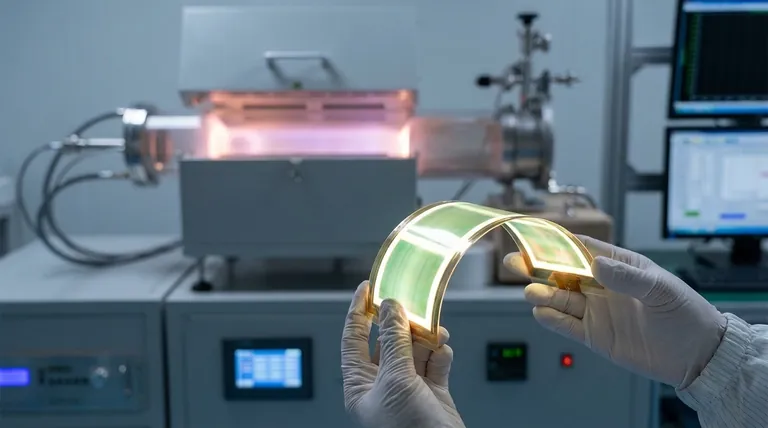
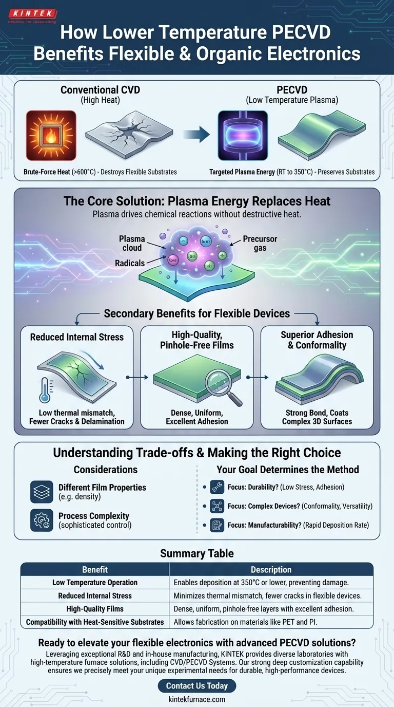
At its core, the lower operating temperature of Plasma-Enhanced Chemical Vapor Deposition (PECVD) is what makes it compatible with the heat-sensitive materials used in flexible and organic electronics. Unlike conventional methods that require extreme heat, PECVD uses an energized plasma to drive chemical reactions, allowing for high-quality film deposition at temperatures low enough to prevent the underlying organic or polymer substrates from melting, warping, or degrading.
The fundamental advantage of PECVD is that it replaces the brute-force energy of high heat with the targeted energy of a plasma. This shift enables the fabrication of advanced electronic devices on materials that simply could not survive traditional manufacturing processes.
The Core Challenge: Thermal Budgets in Modern Electronics
Why Flexible and Organic Substrates Can't Handle Heat
Flexible and organic electronics are often built on polymer-based substrates like polyethylene terephthalate (PET) or polyimide (PI), or use organic semiconductor materials.
These materials have very low melting points and glass transition temperatures compared to traditional silicon wafers. Exposing them to the high temperatures of conventional Chemical Vapor Deposition (CVD)—often exceeding 600°C—would cause irreversible damage, rendering the device useless.
The Problem with High-Temperature Deposition
Traditional CVD relies solely on thermal energy to break down precursor gases and deposit a thin film. This high-heat requirement fundamentally limits its use to thermally robust substrates like silicon or glass.
Applying these methods to a flexible polymer would be like trying to bake a cake on a plastic plate. The substrate would be destroyed long before the deposition process was complete.
How PECVD Solves the Thermal Problem
Plasma: The Key to Low-Temperature Reactions
PECVD circumvents the need for extreme heat by introducing energy in a different form: an electromagnetic field that ignites a plasma.
This plasma is a state of matter containing highly reactive ions and radicals. These energized particles have enough energy to drive the necessary chemical reactions for film deposition without requiring the entire chamber and substrate to be heated to destructive temperatures.
Preserving Substrate Integrity and Performance
By using plasma, PECVD can successfully deposit films at much lower temperatures, typically from room temperature up to 350°C.
This range is safely below the degradation threshold for most polymers and organic materials. This single capability opens the door to creating sophisticated electronic layers on flexible, lightweight, and even transparent substrates.
Beyond Temperature: Secondary Benefits for Flexible Devices
While low temperature is the enabling feature, PECVD offers other critical advantages that make it exceptionally well-suited for flexible electronics.
Reducing Internal Stress
Depositing a film at high temperature onto a cool substrate creates immense internal stress as the materials cool at different rates. This stress leads to cracking and delamination, especially when the device is flexed.
Because PECVD operates at a lower temperature, the thermal mismatch between the deposited film and the flexible substrate is drastically reduced. This results in lower-stress films that are more durable and reliable.
Ensuring High-Quality, Pinhole-Free Films
The energetic plasma process promotes the formation of dense, uniform films with excellent adhesion to the substrate.
This results in fewer pinholes and defects, which is critical for electronic performance. A single pinhole in a dielectric layer can create an electrical short and cause total device failure.
Superior Adhesion and Conformality
PECVD films exhibit very strong adhesion, ensuring the deposited layers do not peel off when the device is bent or twisted.
Furthermore, the process provides excellent "step coverage," meaning it can uniformly coat complex, three-dimensional, and uneven surfaces, which is essential for building intricate, multi-layered device architectures.
Understanding the Trade-offs
No technology is without its compromises. While revolutionary, PECVD has considerations that distinguish it from traditional high-temperature methods.
Film Properties vs. High-Temperature Methods
Films deposited via PECVD can have slightly different properties than those grown at high temperatures. For example, they may have a different density or incorporate elements from the plasma, such as hydrogen.
These properties are not inherently negative—in some cases, creating a "polymer-like" character can be advantageous—but they must be accounted for in the device design. The film is not always a direct 1:1 replacement for its high-temperature counterpart.
Process Complexity and Control
Managing a plasma adds a layer of complexity. The final film's properties are highly dependent on parameters like gas composition, pressure, power, and frequency.
Achieving consistent and repeatable results requires more sophisticated equipment and precise process control compared to simpler thermal CVD methods.
Making the Right Choice for Your Application
Selecting a deposition method depends entirely on your end goal. PECVD is not just a low-temperature alternative; it is a distinct process with a unique combination of benefits.
- If your primary focus is device durability on a flexible substrate: The key benefits are PECVD's low internal stress and superior film adhesion, which prevent cracking and delamination during use.
- If your primary focus is fabricating complex, multi-layered organic devices: The crucial advantages are the excellent conformality for covering uneven features and the versatility to deposit different types of materials.
- If your primary focus is manufacturability and throughput: The rapid deposition rate of PECVD offers a significant speed advantage over many other deposition techniques, enabling faster production cycles.
Ultimately, PECVD is a foundational technology that makes the very concept of high-performance flexible and organic electronics a practical reality.
Summary Table:
| Benefit | Description |
|---|---|
| Low Temperature Operation | Enables deposition at 350°C or lower, preventing damage to polymers and organic materials. |
| Reduced Internal Stress | Minimizes thermal mismatch, leading to fewer cracks and delamination in flexible devices. |
| High-Quality Films | Produces dense, uniform, and pinhole-free layers with excellent adhesion and conformality. |
| Compatibility with Heat-Sensitive Substrates | Allows fabrication on materials like PET and PI, expanding design possibilities. |
Ready to elevate your flexible electronics with advanced PECVD solutions? Leveraging exceptional R&D and in-house manufacturing, KINTEK provides diverse laboratories with high-temperature furnace solutions, including CVD/PECVD Systems. Our strong deep customization capability ensures we precisely meet your unique experimental needs for durable, high-performance devices. Contact us today to discuss how we can support your innovation!
Visual Guide
Related Products
- Slide PECVD Tube Furnace with Liquid Gasifier PECVD Machine
- RF PECVD System Radio Frequency Plasma Enhanced Chemical Vapor Deposition
- Inclined Rotary Plasma Enhanced Chemical Deposition PECVD Tube Furnace Machine
- Inclined Rotary Plasma Enhanced Chemical Deposition PECVD Tube Furnace Machine
- Multi Heating Zones CVD Tube Furnace Machine for Chemical Vapor Deposition Equipment
People Also Ask
- What role does a Tube Furnace play in the CVD growth of carbon nanotubes? Achieve High-Purity CNT Synthesis
- How does a hydrogen reduction environment in an industrial tube furnace facilitate gold-copper alloy microspheres?
- What are the typical conditions for plasma-enhanced CVD processes? Achieve Low-Temperature Thin Film Deposition
- In which industries is the tube furnace commonly used? Essential for Materials Science, Energy, and More
- What is plasma in the context of PECVD? Unlock Low-Temperature Thin Film Deposition


