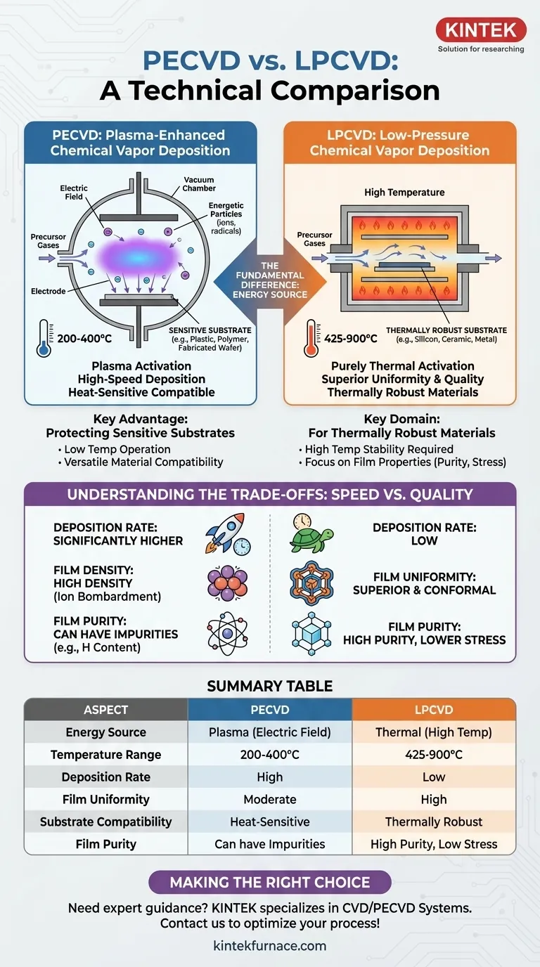
At its core, the primary difference between Plasma-Enhanced Chemical Vapor Deposition (PECVD) and Low-Pressure Chemical Vapor Deposition (LPCVD) is the energy source used to drive the film-forming reaction. PECVD uses an electric field to generate energetic plasma, allowing deposition at low temperatures (200-400°C). In contrast, LPCVD relies solely on high thermal energy (425-900°C) to activate the precursor gases. This single distinction dictates everything from material compatibility to film quality and production speed.
Choosing between these two methods is a fundamental engineering trade-off. PECVD prioritizes processing speed and compatibility with heat-sensitive materials, whereas LPCVD prioritizes film uniformity and quality at the cost of much higher process temperatures.
The Fundamental Difference: How Energy is Supplied
The method used to supply energy to the precursor gases is the defining characteristic that separates PECVD and LPCVD, directly influencing their capabilities and ideal use cases.
PECVD: Plasma-Enhanced Activation
PECVD utilizes an electric field to ionize gases into a plasma within the reaction chamber. This plasma contains highly reactive ions and radicals.
These energized particles bombard the substrate surface, providing the necessary energy for chemical reactions to occur and form a solid film, even at low temperatures.
LPCVD: Purely Thermal Activation
LPCVD relies exclusively on high temperatures to provide the activation energy for the chemical reaction.
The substrate is heated inside a low-pressure furnace, and when precursor gases flow over the hot surface, they decompose and react to deposit the desired film. The low pressure helps ensure the gases diffuse evenly, promoting uniform film growth.
How Temperature Dictates Application
The stark difference in operating temperature is the most critical factor when selecting between the two processes, as it determines which materials can be used as substrates.
PECVD's Advantage: Protecting Sensitive Substrates
The low operating temperature of PECVD (200-400°C) is its key advantage. It allows for the deposition of high-quality films onto materials that cannot withstand high heat.
This includes substrates like plastics, polymers, and fully fabricated semiconductor wafers that already contain metallic interconnects or other temperature-sensitive components. This makes PECVD exceptionally versatile.
LPCVD's Domain: For Thermally Robust Materials
LPCVD is reserved for substrates that are stable at its required high temperatures (425-900°C), such as silicon wafers, ceramics, or certain metals.
The high-temperature process is often chosen when the resulting film properties, such as low stress or high purity, are more critical than the thermal budget of the substrate itself.
Understanding the Trade-offs: Speed vs. Quality
Beyond temperature, the choice between PECVD and LPCVD involves a direct trade-off between manufacturing speed and the final characteristics of the deposited film.
Deposition Rate and Throughput
PECVD generally achieves significantly higher deposition rates. The highly reactive plasma accelerates the chemical kinetics far beyond what is possible with thermal energy alone.
This speed makes PECVD highly suitable for high-throughput manufacturing environments where process time is a critical economic factor, such as in solar cell and flat-panel display production.
Film Uniformity and Conformal Coverage
LPCVD typically produces films with superior uniformity and conformal coverage, especially over complex, non-planar surfaces.
Because the process is not line-of-sight and relies on gas diffusion at low pressure, it can coat intricate 3D topographies more evenly than the more directional plasma-based process of PECVD.
Film Density and Purity
PECVD can produce very dense films due to the constant ion bombardment compacting the film as it grows. However, these films can sometimes have higher hydrogen content or other impurities from the plasma precursors, which may affect electrical properties.
LPCVD films often exhibit higher purity and lower intrinsic stress. The high-temperature environment can help anneal out defects and drive off impurities during the deposition process itself, resulting in a more stable film structure.
Making the Right Choice for Your Process
Your specific goal will determine which deposition technology is the appropriate choice. The decision is a balance between material constraints, desired film properties, and production demands.
- If your primary focus is processing heat-sensitive substrates: PECVD is the clear and often only choice due to its low operating temperatures.
- If your primary focus is achieving the highest film purity and uniformity over complex topography: LPCVD is typically superior, provided your substrate can tolerate the heat.
- If your primary focus is maximizing manufacturing throughput and speed: PECVD offers faster deposition rates, making it more suitable for high-volume production.
- If your primary focus is creating a dense, hard coating: PECVD's ion-assisted deposition can be beneficial for creating dense and mechanically robust films.
Understanding this core trade-off between plasma-driven speed and thermally-driven quality is the key to selecting the right deposition technology for your specific goal.
Summary Table:
| Aspect | PECVD | LPCVD |
|---|---|---|
| Energy Source | Plasma (electric field) | Thermal (high temperature) |
| Temperature Range | 200-400°C | 425-900°C |
| Deposition Rate | High | Low |
| Film Uniformity | Moderate | High |
| Substrate Compatibility | Heat-sensitive materials (e.g., plastics, polymers) | Thermally robust materials (e.g., silicon, ceramics) |
| Film Purity | Can have impurities (e.g., hydrogen) | High purity, low stress |
Need expert guidance on selecting the right CVD system for your lab? At KINTEK, we specialize in advanced high-temperature furnace solutions, including CVD/PECVD Systems. Leveraging our exceptional R&D and in-house manufacturing, we offer deep customization to precisely meet your unique experimental requirements, whether you're working with heat-sensitive substrates or demanding high film quality. Contact us today to optimize your deposition process and boost efficiency!
Visual Guide
Related Products
- Slide PECVD Tube Furnace with Liquid Gasifier PECVD Machine
- RF PECVD System Radio Frequency Plasma Enhanced Chemical Vapor Deposition
- Inclined Rotary Plasma Enhanced Chemical Deposition PECVD Tube Furnace Machine
- Inclined Rotary Plasma Enhanced Chemical Deposition PECVD Tube Furnace Machine
- Multi Heating Zones CVD Tube Furnace Machine for Chemical Vapor Deposition Equipment
People Also Ask
- How does PECVD equipment contribute to TOPCon bottom cells? Mastering Hydrogenation for Maximum Solar Efficiency
- What plasma source is used in PE-CVD tube furnaces? Unlock Low-Temperature, High-Quality Deposition
- What is plasma in the context of PECVD? Unlock Low-Temperature Thin Film Deposition
- What are the main advantages of PECVD tube furnaces compared to CVD tube furnaces? Lower Temp, Faster Deposition, and More
- How does a hydrogen reduction environment in an industrial tube furnace facilitate gold-copper alloy microspheres?


