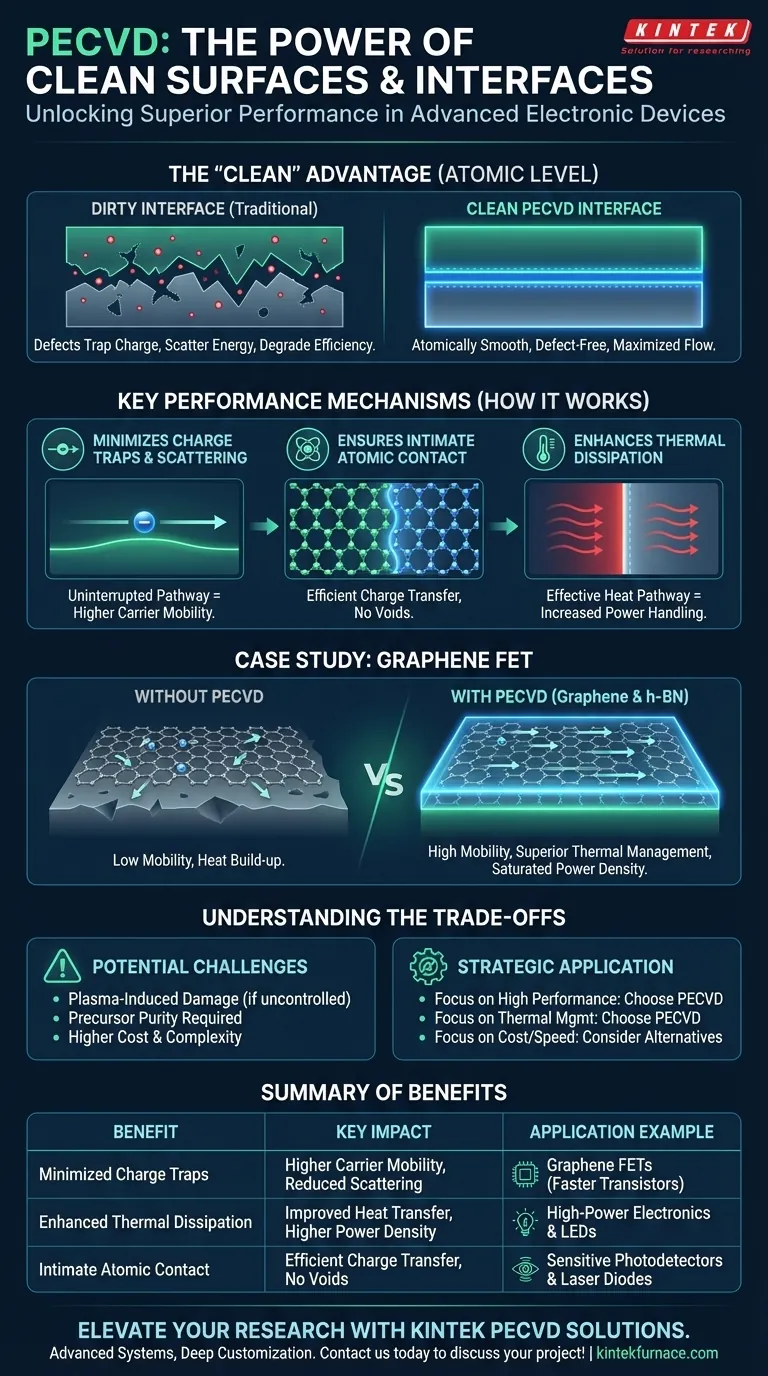
In essence, the exceptionally clean surfaces and interfaces created by Plasma-Enhanced Chemical Vapor Deposition (PECVD) directly translate to superior performance in advanced electronic devices. This is achieved by minimizing defects that would otherwise trap charge carriers, scatter energy, and degrade device efficiency. The result is measurably higher carrier mobility and increased power handling capabilities, as seen in materials like graphene and hexagonal boron nitride (h-BN).
The fundamental advantage of PECVD-prepared interfaces is the reduction of electronic and thermal barriers. By creating atomically clean and well-bonded junctions, PECVD allows electrons and heat to move more freely across material layers, unlocking the true performance potential of the device.
The Physics of a 'Clean' Interface
A "clean" interface in semiconductor fabrication is not merely about the absence of dust. It refers to a near-perfect junction at the atomic level, which PECVD is uniquely capable of producing. This structural integrity is the source of its performance benefits.
Minimizing Charge Traps and Scattering
Any impurity, atomic vacancy, or structural imperfection at the interface between two materials acts as a roadblock for electrons. These defects can either trap charge carriers, effectively removing them from operation, or scatter them, forcing them to take a less direct path.
A clean interface formed by PECVD is atomically smooth and free of these contaminants. This creates an uninterrupted pathway, allowing charge carriers to flow with minimal resistance.
Ensuring Intimate Atomic Contact
The energetic nature of the PECVD process ensures that deposited atoms have enough mobility on the surface to find their ideal lattice sites. This results in a dense, conformal film with no voids or gaps at the interface.
This intimate contact is critical for ensuring efficient charge transfer between layers and for establishing a seamless path for heat dissipation.
Enhancing Thermal Dissipation
High-power electronic devices generate significant heat in very small active regions. This heat must be conducted away efficiently to prevent performance degradation or device failure.
An interface with gaps or impurities acts as a significant barrier to heat transfer. The clean, closely contacted interfaces produced by PECVD provide an excellent thermal pathway, allowing phonons (the primary carriers of heat in a solid) to move easily away from the active area.
Performance Gains: The Graphene FET Case Study
The benefits of clean PECVD interfaces are not theoretical. They are clearly demonstrated in the fabrication of next-generation devices like graphene-based field-effect transistors (FETs).
The Impact on Carrier Mobility
Carrier mobility is a measure of how quickly an electron can move through a material under an electric field. Higher mobility is a direct requirement for faster, more efficient transistors.
In a graphene FET, the clean interface created by PECVD prevents the scattering of electrons moving through the graphene channel. This directly results in the high mobilities observed in these devices.
The Role of the h-BN Dielectric Layer
When hexagonal boron nitride (h-BN) is used as a dielectric layer alongside graphene, the benefits are amplified. h-BN is an excellent insulator and is structurally very similar to graphene, allowing for a near-perfect, lattice-matched interface.
Using PECVD to deposit the h-BN layer ensures this interface is atomically clean. This combination not only improves carrier mobility but also enhances saturated power density by providing superior electrical insulation and, crucially, a highly efficient path for thermal dissipation.
Understanding the Trade-offs
While powerful, PECVD is not a universal solution. An objective evaluation requires understanding its potential downsides.
Plasma-Induced Damage
The high-energy plasma that defines the PECVD process can, if not perfectly controlled, cause damage to the underlying substrate. This can introduce its own set of defects, partially negating the benefits of the clean deposition. Careful optimization of plasma power, pressure, and chemistry is critical to mitigate this risk.
Precursor Purity and Contamination
The quality of a PECVD film is only as good as the precursor gases used to create it. Any impurities in the source gases can become incorporated into the final film, contaminating the very interface you are trying to keep clean. This demands a significant investment in ultra-high-purity gas handling systems.
Process Complexity and Cost
PECVD is a vacuum-based deposition technique that requires sophisticated, expensive equipment and precise process control. Compared to simpler methods like thermal evaporation or sputtering, it represents a higher barrier to entry in terms of both capital investment and operational expertise.
How to Apply This to Your Project
Your choice of deposition method should be driven by the specific performance goals of your device.
- If your primary focus is maximizing electronic performance: PECVD is a superior choice for creating the defect-free interfaces required for high-mobility transistors, sensitive photodetectors, and other high-performance electronics.
- If your primary focus is thermal management for high-power devices: The ability of PECVD to create thermally conductive, void-free interfaces makes it an indispensable tool for managing heat in power transistors, LEDs, and laser diodes.
- If your primary focus is rapid prototyping or cost-sensitive applications: Simpler methods may be sufficient, but you must be prepared to accept a performance penalty resulting from less-than-perfect material interfaces.
Ultimately, leveraging PECVD is a strategic decision to invest in the quality of the interface, directly enabling next-generation device performance.
Summary Table:
| Benefit | Key Impact | Application Example |
|---|---|---|
| Minimized Charge Traps | Higher carrier mobility, reduced scattering | Graphene FETs for faster transistors |
| Enhanced Thermal Dissipation | Improved heat transfer, higher power density | High-power electronics and LEDs |
| Intimate Atomic Contact | Efficient charge transfer, no voids | Sensitive photodetectors and laser diodes |
Ready to elevate your lab's capabilities with high-performance PECVD solutions? KINTEK leverages exceptional R&D and in-house manufacturing to provide advanced high-temperature furnace systems, including CVD/PECVD Systems, Muffle, Tube, Rotary Furnaces, and Vacuum & Atmosphere Furnaces. Our strong deep customization capability ensures we precisely meet your unique experimental needs, helping you achieve superior device performance with clean, defect-free interfaces. Contact us today to discuss how we can support your project!
Visual Guide
Related Products
- Slide PECVD Tube Furnace with Liquid Gasifier PECVD Machine
- RF PECVD System Radio Frequency Plasma Enhanced Chemical Vapor Deposition
- Inclined Rotary Plasma Enhanced Chemical Deposition PECVD Tube Furnace Machine
- Inclined Rotary Plasma Enhanced Chemical Deposition PECVD Tube Furnace Machine
- Multi Heating Zones CVD Tube Furnace Machine for Chemical Vapor Deposition Equipment
People Also Ask
- How does a hydrogen reduction environment in an industrial tube furnace facilitate gold-copper alloy microspheres?
- What plasma source is used in PE-CVD tube furnaces? Unlock Low-Temperature, High-Quality Deposition
- What are the advantages of using a tube furnace CVD system for Cu(111)/graphene? Superior Scalability and Quality
- What are the main advantages of PECVD tube furnaces compared to CVD tube furnaces? Lower Temp, Faster Deposition, and More
- How does PECVD equipment contribute to TOPCon bottom cells? Mastering Hydrogenation for Maximum Solar Efficiency


