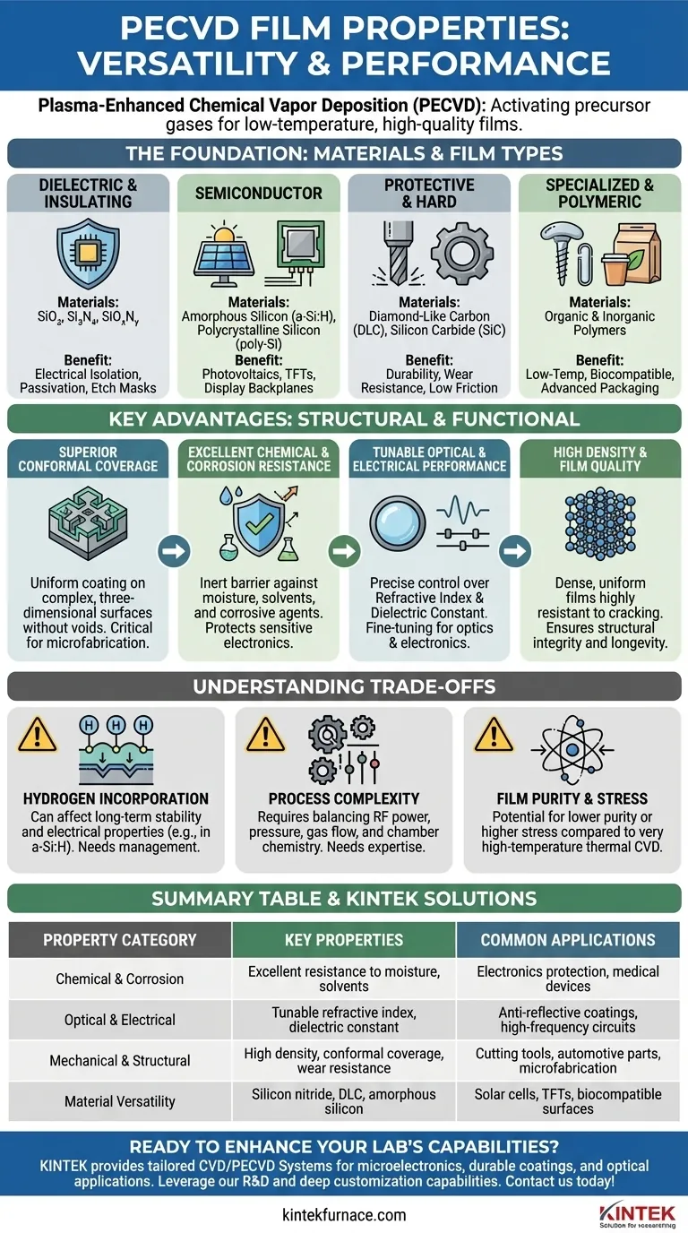
In essence, films deposited by PECVD exhibit a uniquely broad range of properties, from excellent chemical resistance and durability to finely tuned optical and electrical characteristics. This versatility stems from its ability to create high-quality films like silicon nitride, silicon dioxide, and Diamond-Like Carbon (DLC) with superior three-dimensional coverage, even at low temperatures.
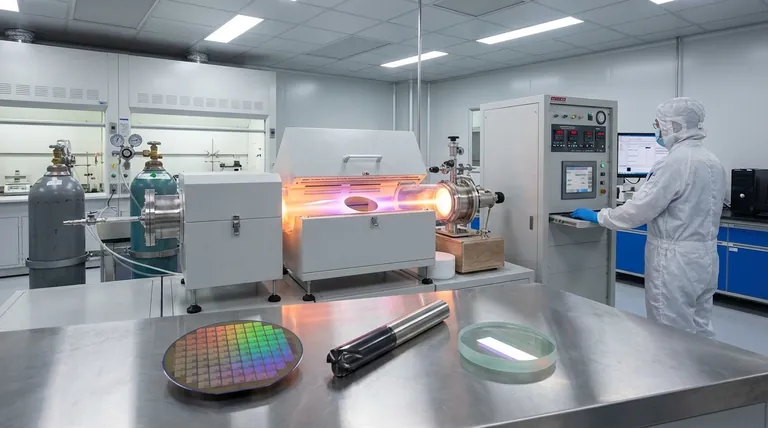
The core advantage of Plasma-Enhanced Chemical Vapor Deposition (PECVD) is its use of a plasma to activate precursor gases. This enables the deposition of high-performance, uniform films at temperatures low enough to be compatible with sensitive substrates like plastics and fully-fabricated microchips.
The Foundation: What Materials Can PECVD Deposit?
The properties a film exhibits are directly tied to the material being deposited. PECVD is known for its ability to handle a wide variety of precursors to create functionally distinct films.
Dielectric and Insulating Films
These are the most common films in microelectronics, used for electrical insulation, passivation layers, and as etch masks.
Key materials include Silicon Dioxide (SiO2), Silicon Nitride (Si3N4), and Silicon Oxynitride (SiOxNy). They provide excellent electrical isolation and protect underlying circuits.
Semiconductor Films
PECVD is crucial for depositing semiconductor layers, particularly in photovoltaics and thin-film transistors (TFTs).
The primary material here is Amorphous Silicon (a-Si:H), a key component in solar cells and display backplanes. The process can also be used for polycrystalline silicon (poly-Si).
Protective and Hard Coatings
For applications requiring high durability, wear resistance, and low friction, PECVD is a leading choice.
Diamond-Like Carbon (DLC) films provide a hard, slick surface ideal for cutting tools, automotive parts, and biomedical implants. Silicon Carbide (SiC) also offers exceptional hardness and thermal stability.
Specialized and Polymeric Films
The low-temperature nature of PECVD opens the door to depositing materials that cannot withstand traditional high-temperature methods.
This includes depositing organic and inorganic polymers for applications like advanced food packaging or creating biocompatible surfaces on medical devices.
Key Film Properties and Their Advantages
The PECVD process itself imparts desirable structural and functional characteristics to the deposited films, often surpassing what is possible with other methods like Physical Vapor Deposition (PVD).
Superior Conformal Coverage
PECVD excels at depositing films that uniformly coat complex, three-dimensional surfaces without voids or thinning at the corners.
This conformal step coverage is critical in microfabrication, ensuring complete insulation and protection over the intricate topography of integrated circuits.
Excellent Chemical and Corrosion Resistance
Films like silicon nitride and DLC are inherently inert, creating an outstanding barrier against moisture, solvents, and other corrosive agents.
This property makes PECVD coatings ideal for protecting sensitive electronics, medical instruments, and components operating in harsh environments.
Tunable Optical and Electrical Performance
The plasma process allows for precise control over film composition, density, and microstructure.
This enables the fine-tuning of properties like refractive index for anti-reflective coatings in optics, or dielectric constant for optimal insulation in high-frequency electronics.
High Density and Film Quality
PECVD produces dense, uniform films that are highly resistant to cracking.
This structural integrity ensures reliability and longevity, preventing defects that could lead to device failure.
Understanding the Trade-offs
While powerful, PECVD is not a universal solution. Understanding its limitations is key to making an informed decision. The plasma that provides its core benefits also introduces complexities.
Hydrogen Incorporation
Many PECVD processes use hydrogen-containing precursors (e.g., silane, ammonia). This can lead to hydrogen being incorporated into the final film, such as in a-Si:H.
While sometimes desirable, this incorporated hydrogen can affect the film's long-term stability and electrical properties, a factor that must be managed.
Process Complexity
Controlling a plasma environment is more complex than controlling a simple thermal or evaporation process.
Factors like RF power, pressure, gas flow rates, and chamber chemistry must be precisely balanced to achieve repeatable, high-quality results. This often requires more sophisticated equipment and process expertise.
Film Purity and Stress
Compared to very high-temperature thermal CVD, PECVD films can sometimes have lower purity or higher intrinsic stress due to the energetic ion bombardment from the plasma.
This trade-off is often acceptable, as the benefit of low-temperature deposition outweighs the slight difference in film perfection for most applications.
Making the Right Choice for Your Application
Selecting a deposition method depends entirely on the required film properties and the constraints of your substrate.
- If your primary focus is microelectronics manufacturing: PECVD is the industry standard for depositing high-quality dielectric insulators (SiO2, Si3N4) over sensitive components because of its low-temperature, high-coverage process.
- If your primary focus is creating durable surface coatings: PECVD is a leading choice for wear-resistant films like Diamond-Like Carbon (DLC) on tools, mechanical parts, or medical implants.
- If your primary focus is advanced optics or photovoltaics: The ability to tune refractive index and deposit materials like amorphous silicon makes PECVD a critical and indispensable tool.
By understanding its unique plasma-driven mechanism, you can leverage PECVD to engineer films with precisely the properties your application demands.
Summary Table:
| Property Category | Key Properties | Common Applications |
|---|---|---|
| Chemical & Corrosion | Excellent resistance to moisture, solvents | Electronics protection, medical devices |
| Optical & Electrical | Tunable refractive index, dielectric constant | Anti-reflective coatings, high-frequency circuits |
| Mechanical & Structural | High density, conformal coverage, wear resistance | Cutting tools, automotive parts, microfabrication |
| Material Versatility | Silicon nitride, DLC, amorphous silicon | Solar cells, TFTs, biocompatible surfaces |
Ready to enhance your lab's capabilities with advanced PECVD solutions? Leveraging exceptional R&D and in-house manufacturing, KINTEK provides diverse laboratories with tailored high-temperature furnace systems, including our specialized CVD/PECVD Systems. Our strong deep customization capability ensures we precisely meet your unique experimental needs, whether for microelectronics, durable coatings, or optical applications. Contact us today to discuss how our expertise can drive your innovations forward!
Visual Guide
Related Products
- RF PECVD System Radio Frequency Plasma Enhanced Chemical Vapor Deposition
- Slide PECVD Tube Furnace with Liquid Gasifier PECVD Machine
- Inclined Rotary Plasma Enhanced Chemical Deposition PECVD Tube Furnace Machine
- Inclined Rotary Plasma Enhanced Chemical Deposition PECVD Tube Furnace Machine
People Also Ask
- What are the applications of plasma enhanced chemical vapor deposition? Key Uses in Electronics, Optics & Materials
- What is PECVD specification? A Guide to Choosing the Right System for Your Lab
- How is silicon dioxide deposited from tetraethylorthosilicate (TEOS) in PECVD? Achieve Low-Temperature, High-Quality SiO2 Films
- What is the role of RF power in PECVD and how does the RF-PECVD process work? Master Thin Film Deposition Control
- What are some promising applications of PECVD-prepared 2D materials? Unlock Advanced Sensing and Optoelectronics


