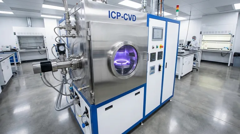
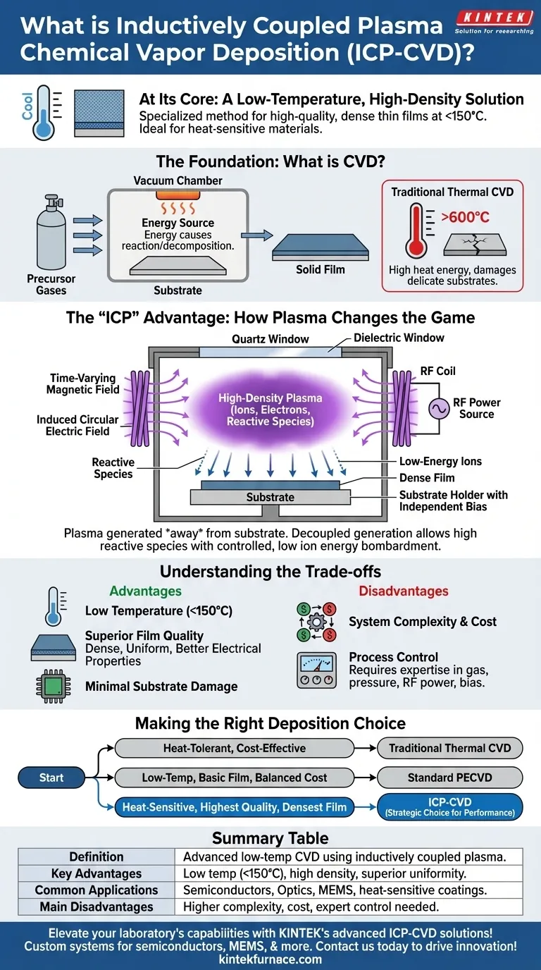
At its core, Inductively Coupled Plasma Chemical Vapor Deposition (ICP-CVD) is a specialized, low-temperature method for creating high-quality, dense thin films on a substrate. It is an advanced form of Chemical Vapor Deposition (CVD) that uses a high-density plasma, generated by an electromagnetic field, to drive the chemical reactions necessary for deposition. This process allows for film creation at temperatures often below 150°C, making it ideal for heat-sensitive materials.
The essential value of ICP-CVD is its ability to create a very dense, reactive plasma at low pressure without directly heating or bombarding the substrate. This enables the deposition of exceptionally high-quality films on materials that cannot withstand the high temperatures of traditional deposition methods.
First, Understanding the Foundation: What is CVD?
To grasp ICP-CVD, one must first understand the general principle of Chemical Vapor Deposition (CVD).
The Core Process: Gas to Solid Film
CVD is a manufacturing process used to apply thin, solid coatings onto a surface, known as a substrate.
It begins by introducing one or more precursor gases into a vacuum chamber. These gases contain the atoms that will make up the final film.
Energy is then applied, causing the precursor gases to react or decompose. The resulting solid material deposits onto all exposed surfaces inside the chamber, forming a thin, uniform film.
The Role of Energy
The critical factor in any CVD process is the energy source used to break down the precursor gases.
Traditionally, this energy is thermal. In Thermal CVD, the substrate is heated to very high temperatures (often >600°C), which provides the energy for the chemical reactions to occur on its surface.
However, many advanced applications use substrates (like polymers or complex microchips) that would be damaged or destroyed by such high heat. This limitation led to the development of plasma-based techniques.
The "ICP" Advantage: How Plasma Changes the Game
Plasma-Enhanced CVD (PECVD) is a broad category of techniques that use an electric or magnetic field to turn the precursor gas into a plasma, enabling deposition at much lower temperatures. ICP-CVD is a highly advanced form of PECVD.
What is a Plasma?
Often called the "fourth state of matter," a plasma is an ionized gas. It is a high-energy soup of ions, electrons, and highly reactive neutral species.
These reactive species can undergo the chemical reactions needed for film deposition at room temperature, eliminating the need for extreme substrate heat.
How the "Inductively Coupled" Mechanism Works
Standard PECVD systems create plasma directly between two electrodes, with the substrate sitting on one of them. This can lead to high-energy ion bombardment that can damage the substrate or the growing film.
ICP-CVD solves this with a more elegant approach. An RF (radio frequency) power source is connected to a coil wrapped around a dielectric (e.g., quartz) chamber window.
This RF power creates a time-varying magnetic field, which in turn induces a circular electric field inside the chamber. This electric field energizes and ionizes the gas, creating a very dense, stable plasma.
Crucially, the plasma is generated away from the substrate, and the substrate itself can be independently biased. This decouples plasma generation from the substrate conditions, allowing for a high density of reactive species with low, controlled ion energy hitting the surface.
Understanding the Trade-offs of ICP-CVD
Like any specialized technology, ICP-CVD involves a distinct set of advantages and disadvantages that define its use.
Advantage: Low Temperature, High Quality
This is the primary reason for its existence. The ability to deposit dense, low-stress films of materials like silicon dioxide (SiO₂) and silicon nitride (Si₃N₄) at temperatures below 150°C is invaluable for producing complex semiconductor devices, optics, and MEMS.
Advantage: Superior Film Properties
The high-density plasma generated by the inductive coil leads to films that are denser, more uniform, and have better electrical properties (e.g., lower leakage current) than those deposited by simpler, lower-density plasma methods.
Disadvantage: System Complexity and Cost
The hardware required for ICP-CVD—including the RF coil, impedance matching network, high-quality vacuum chamber, and power supplies—is significantly more complex and expensive than that for thermal CVD or standard PECVD systems.
Disadvantage: Process Control
While powerful, the decoupling of plasma generation and substrate bias adds more process variables that must be carefully controlled. Optimizing a process for a specific film requires significant expertise in managing gas flows, pressure, RF power to the coil, and substrate bias.
Making the Right Deposition Choice
Your choice of deposition technology depends entirely on the technical requirements of your film and the thermal budget of your substrate.
- If your primary focus is cost-effectiveness for a heat-tolerant substrate: Traditional thermal CVD is often the most straightforward and economical choice.
- If your primary focus is depositing a basic film at low temperatures without needing the absolute highest density: A standard, parallel-plate PECVD system offers a good balance of performance and cost.
- If your primary focus is depositing the highest quality, densest film possible on a highly temperature-sensitive or delicate substrate: ICP-CVD is the definitive technical choice, justifying its higher complexity and cost.
Ultimately, selecting ICP-CVD is a strategic decision to prioritize superior film properties and substrate integrity above all else.
Summary Table:
| Aspect | Description |
|---|---|
| Definition | Advanced CVD method using inductively coupled plasma for low-temperature thin film deposition. |
| Key Advantages | Low-temperature operation (<150°C), high film density, superior uniformity, and minimal substrate damage. |
| Common Applications | Semiconductor devices, optics, MEMS, and other heat-sensitive material coatings. |
| Main Disadvantages | Higher system complexity, increased cost, and need for expert process control. |
Elevate your laboratory's capabilities with KINTEK's advanced ICP-CVD solutions! Leveraging exceptional R&D and in-house manufacturing, we provide high-temperature furnace systems like Muffle, Tube, Rotary, Vacuum & Atmosphere Furnaces, and CVD/PECVD Systems, tailored to your unique needs. Our deep customization ensures precise performance for applications in semiconductors, MEMS, and beyond. Contact us today to discuss how we can enhance your deposition processes and drive innovation in your projects!
Visual Guide
Related Products
- HFCVD Machine System Equipment for Drawing Die Nano Diamond Coating
- Cylindrical Resonator MPCVD Machine System for Lab Diamond Growth
- Custom Made Versatile CVD Tube Furnace Chemical Vapor Deposition CVD Equipment Machine
- RF PECVD System Radio Frequency Plasma Enhanced Chemical Vapor Deposition
- Inclined Rotary Plasma Enhanced Chemical Deposition PECVD Tube Furnace Machine
People Also Ask
- What is the significance of the vacuum pressure control system in the CVD coating process for powders?
- What are the equipment for chemical vapor deposition? A Guide to the 5 Essential Components
- What materials are commonly used in CVD coating systems? Explore Key Materials for Superior Coatings
- What is Hot-filament Chemical Vapor Deposition (HFCVD)? Achieve High-Quality Thin Films with Precision Control
- What is the function of high-purity Argon (Ar) gas during CVD? Optimize Your Thin Film Uniformity and Purity


