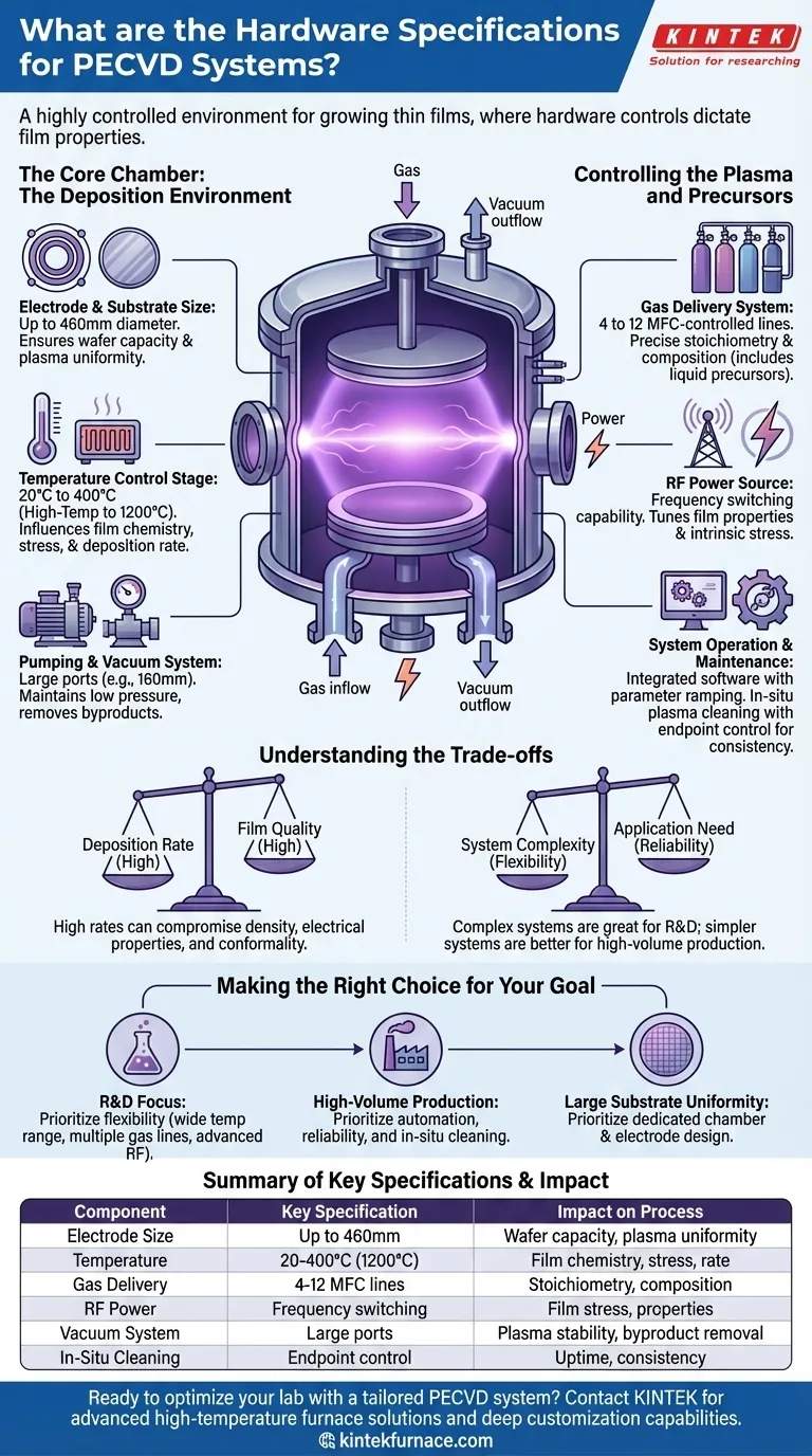
At its core, a PECVD system is a highly controlled environment for growing thin films. Its hardware specifications revolve around a vacuum chamber, a radio-frequency (RF) power source to create plasma, a gas delivery system for precursor chemicals, and a heated stage to hold the substrate. Key specifications include electrode sizes ranging from 240mm to 460mm, substrate temperature control from 20°C to over 400°C, and precise gas delivery through 4 to 12 mass-flow-controlled (MFC) lines.
The specific hardware specifications of a PECVD system are not just a list of features; they are a set of controls. The true value lies in understanding how these components work together to manipulate the plasma environment and, ultimately, dictate the final properties of the deposited film.
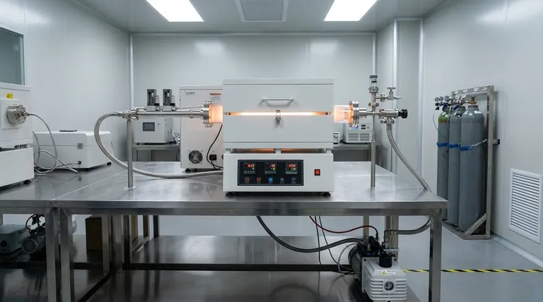
The Core Reaction Chamber: The Deposition Environment
The process chamber is where the chemical reaction takes place. Its design and components are foundational to the system's capabilities, directly influencing wafer capacity, temperature uniformity, and film quality.
Electrode and Substrate Size
The size of the electrodes and the substrate stage determines the maximum wafer size the system can handle. Common specifications accommodate substrates up to 460mm in diameter.
Larger electrodes are essential for ensuring uniform plasma distribution over the entire substrate, which is critical for consistent film thickness and properties across the wafer.
Temperature Control Stage
The substrate holder, or stage, is actively heated. A standard temperature range is typically 20°C to 400°C, with high-temperature options available that can reach up to 1200°C.
Temperature is a primary lever for controlling film chemistry, deposition rate, and intrinsic stress. The ability to precisely control and ramp this temperature is a key hardware function.
Pumping and Vacuum System
A robust vacuum system, often connected via a large port (e.g., 160mm), is required to reduce the chamber pressure. This low-pressure environment is necessary to ignite and sustain the plasma.
It also serves to efficiently remove reaction byproducts, preventing contamination and ensuring a pure deposition process.
Controlling the Plasma and Precursors
The quality of a PECVD film is determined by the precise control of its two main inputs: the chemical precursors and the plasma energy that breaks them down.
Gas Delivery System
Precursor gases, dopants, and cleaning gases are delivered into the chamber through a gas pod. These systems typically feature 4, 8, or 12 individual gas lines.
Each line is governed by a Mass Flow Controller (MFC), an essential component that ensures an exact and repeatable flow rate of gas, which directly translates to control over the film's stoichiometry and composition. This includes handling both standard gases and vapor from liquid precursors.
Radio Frequency (RF) Power Source
An RF generator supplies the energy needed to dissociate the precursor gases and create plasma. A key feature is the ability to use different frequencies or to switch between them.
This RF switching is a powerful tool for process tuning. It allows for direct manipulation and control over the deposited film's properties, most notably its intrinsic stress.
System Operation and Maintenance
Modern PECVD systems are designed for repeatability and ease of use, incorporating software and hardware features that streamline both the deposition process and routine maintenance.
Control Systems and Software
Operations are typically managed through an integrated computer with a touchscreen interface. This allows operators to run pre-programmed recipes with high precision.
Advanced parameter ramping software enables gradual changes in process conditions like temperature or gas flow during a run, which is crucial for creating complex, multi-layer film stacks or graded interfaces.
In-Situ Plasma Cleaning
Over time, deposition occurs on all internal chamber surfaces, not just the wafer. To ensure run-to-run consistency, the chamber must be cleaned regularly.
High-end systems feature in-situ plasma cleaning, which uses a reactive gas plasma (like NF₃ or SF₆) to etch away unwanted deposits without breaking vacuum. The inclusion of endpoint control automatically stops the cleaning process once the chamber is clean, preventing damage and maximizing uptime.
Understanding the Trade-offs
Choosing a PECVD system involves balancing competing priorities. The "best" hardware is entirely dependent on the intended application.
Deposition Rate vs. Film Quality
A "fast deposition rate" is often advertised as a key benefit. This is typically achieved with higher power, higher pressure, or higher precursor flow rates.
However, high rates can come at the cost of film quality. Rapid deposition can lead to lower film density, higher hydrogen content, poorer electrical properties, and less conformal step coverage. Achieving high-quality films often requires a slower, more controlled process.
System Complexity vs. Application Need
A system with 12 gas lines, dual-frequency RF, and a 1200°C temperature range offers incredible flexibility for research and development.
However, this complexity adds significant cost and maintenance overhead. For a dedicated production process running the same film repeatedly, a simpler, more robust system with fewer variables is often the more reliable and cost-effective choice.
Making the Right Choice for Your Goal
Your hardware requirements should be driven by the properties of the film you need to create.
- If your primary focus is research and development: Prioritize flexibility. A system with a wide temperature range, multiple gas lines, and advanced RF control for stress tuning is essential.
- If your primary focus is high-volume production: Prioritize automation, reliability, and low cost-of-ownership. Features like robust in-situ cleaning with endpoint control and stable, simplified process controls are critical.
- If your primary focus is depositing highly uniform films on large substrates: Prioritize a chamber and electrode design specifically engineered for your wafer size to ensure excellent plasma and temperature uniformity.
Ultimately, the hardware specifications are the tools you use to define the process and achieve the desired outcome for your material.
Summary Table:
| Component | Key Specification | Impact on Process |
|---|---|---|
| Electrode Size | Up to 460mm diameter | Determines wafer capacity and plasma uniformity |
| Temperature Control | 20°C to 400°C (up to 1200°C) | Influences film chemistry, stress, and deposition rate |
| Gas Delivery | 4 to 12 MFC-controlled lines | Ensures precise stoichiometry and composition control |
| RF Power Source | Frequency switching capability | Allows tuning of film stress and properties |
| Vacuum System | Large ports (e.g., 160mm) | Maintains plasma stability and removes byproducts |
| In-Situ Cleaning | Plasma cleaning with endpoint control | Enhances uptime and run-to-run consistency |
Ready to optimize your lab with a tailored PECVD system? At KINTEK, we leverage exceptional R&D and in-house manufacturing to provide advanced high-temperature furnace solutions, including CVD/PECVD Systems. Our deep customization capabilities ensure your unique experimental requirements are met precisely—boosting efficiency and reliability. Contact us today to discuss how our expertise can enhance your thin film deposition processes!
Visual Guide
Related Products
- RF PECVD System Radio Frequency Plasma Enhanced Chemical Vapor Deposition
- Slide PECVD Tube Furnace with Liquid Gasifier PECVD Machine
- Inclined Rotary Plasma Enhanced Chemical Deposition PECVD Tube Furnace Machine
- Inclined Rotary Plasma Enhanced Chemical Deposition PECVD Tube Furnace Machine
- Cylindrical Resonator MPCVD Machine System for Lab Diamond Growth
People Also Ask
- How is silicon dioxide deposited from tetraethylorthosilicate (TEOS) in PECVD? Achieve Low-Temperature, High-Quality SiO2 Films
- What are the applications of plasma enhanced chemical vapor deposition? Key Uses in Electronics, Optics & Materials
- What are the advantages of PECVD in film deposition? Achieve Low-Temp, High-Quality Coatings
- How are deposition rates and film properties controlled in PECVD? Master Key Parameters for Optimal Thin Films
- What is PECVD specification? A Guide to Choosing the Right System for Your Lab


