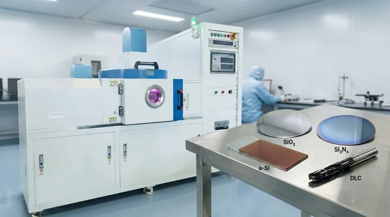
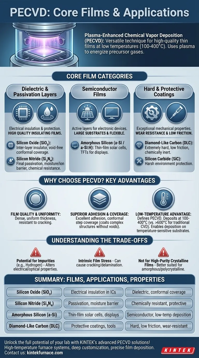
At its core, Plasma-Enhanced Chemical Vapor Deposition (PECVD) is a highly versatile technique primarily used to deposit critical dielectric and semiconductor thin films. The most common materials include silicon oxide (SiO₂), silicon nitride (Si₃N₄), amorphous silicon (a-Si), and diamond-like carbon (DLC), which are fundamental building blocks in microelectronics and optics.
PECVD's true significance isn't just the variety of films it can create, but its ability to deposit them at lower temperatures. This allows for the fabrication of high-quality, uniform, and adherent layers on substrates that cannot withstand the high heat of traditional deposition methods.
The Core Film Categories of PECVD
PECVD is not a one-size-fits-all solution; its use is concentrated on specific categories of materials where its unique process advantages—using a plasma to energize precursor gases—provide a distinct benefit.
Dielectric and Passivation Layers
The most common application of PECVD is for depositing high-quality insulating films. These layers are critical for electrically isolating components and protecting device surfaces.
Silicon Oxide (SiO₂) is a fundamental dielectric used as an insulator between metal layers in integrated circuits. PECVD allows for void-free deposition that conforms to complex surface topographies.
Silicon Nitride (Si₃N₄) is valued for its excellent chemical resistance and ability to act as a barrier against moisture and ion diffusion. It's frequently used as a final passivation layer to protect chips from the environment.
Semiconductor Films
PECVD is also instrumental in creating the active layers for certain electronic devices, particularly those built on large or flexible substrates.
Amorphous Silicon (a-Si), often hydrogenated (a-Si:H), is a key material deposited by PECVD for thin-film solar cells and the transistors used in large-area displays (like LCD screens).
Hard and Protective Coatings
The energetic plasma process can create films with exceptional mechanical properties, making them suitable for protective applications.
Diamond-Like Carbon (DLC) is a class of amorphous carbon material with some of the valuable properties of diamond. These films are extremely hard, have a low coefficient of friction, and are chemically inert, making them ideal coatings for tools, medical implants, and wear-resistant components.
Silicon Carbide (SiC) is another hard and chemically resistant material deposited by PECVD for protective coatings in harsh environments.
Why Choose PECVD for These Materials?
The decision to use PECVD over other methods like Physical Vapor Deposition (PVD) or standard Chemical Vapor Deposition (CVD) is driven by the unique quality and process benefits it offers.
Film Quality and Uniformity
PECVD is renowned for producing films that are dense, uniform in thickness, and resistant to cracking. The plasma-assisted reaction creates a stable and controllable growth environment.
Superior Adhesion and Coverage
Films deposited via PECVD exhibit excellent adhesion to the underlying substrate. The process also provides outstanding conformal step coverage, meaning it can uniformly coat intricate, three-dimensional structures without creating voids or gaps.
The Low-Temperature Advantage
This is the defining benefit of PECVD. Traditional CVD requires very high temperatures (often >600°C) to break down precursor gases. PECVD uses an energy-rich plasma to achieve this, allowing deposition to occur at much lower temperatures (typically 100-400°C).
This low-temperature process is essential for depositing films onto substrates that have already been partially processed or are made of materials with low melting points, such as polymers.
Understanding the Trade-offs
While powerful, PECVD is not without its limitations. Understanding these trade-offs is key to using the technique effectively.
Potential for Impurities
The plasma environment means that fragments of the precursor gases, particularly hydrogen, can be incorporated into the growing film. While sometimes intentional (as in a-Si:H), these impurities can alter the film's electrical or optical properties in unintended ways.
Intrinsic Film Stress
PECVD films often possess a built-in mechanical stress (either tensile or compressive). If not properly managed, high stress can cause the film to crack or delaminate from the substrate, leading to device failure.
Not Ideal for High-Purity Crystalline Films
While excellent for amorphous or polycrystalline films, PECVD is generally not the preferred method for depositing high-purity, single-crystal films. Techniques like Molecular Beam Epitaxy (MBE) or specialized CVD processes are better suited for that goal.
Making the Right Choice for Your Goal
Your choice of film is dictated entirely by the problem you need to solve. PECVD provides a toolbox of materials suited for specific engineering challenges.
- If your primary focus is electrical insulation or device passivation: Your go-to materials will be silicon oxide (SiO₂) and silicon nitride (Si₃N₄).
- If your primary focus is thin-film solar cells or display backplanes: You will primarily use amorphous silicon (a-Si:H).
- If your primary focus is creating hard, wear-resistant, or low-friction surfaces: Diamond-like carbon (DLC) is the most effective choice.
- If your primary focus is a protective barrier in harsh chemical or thermal environments: Silicon nitride (Si₃N₄) or silicon carbide (SiC) are strong candidates.
Ultimately, PECVD's ability to create high-quality functional films at low temperatures makes it an indispensable process in modern manufacturing.
Summary Table:
| Film Type | Key Applications | Key Properties |
|---|---|---|
| Silicon Oxide (SiO₂) | Electrical insulation in ICs | Dielectric, conformal coverage |
| Silicon Nitride (Si₃N₄) | Passivation, moisture barrier | Chemically resistant, protective |
| Amorphous Silicon (a-Si) | Thin-film solar cells, displays | Semiconductor, low-temperature deposition |
| Diamond-Like Carbon (DLC) | Protective coatings, tools | Hard, low friction, wear-resistant |
| Silicon Carbide (SiC) | Harsh environment protection | Hard, chemically inert |
Unlock the full potential of your lab with KINTEK's advanced PECVD solutions! Leveraging exceptional R&D and in-house manufacturing, we provide diverse laboratories with high-temperature furnace systems like CVD/PECVD Systems, tailored to your unique experimental needs. Our deep customization capabilities ensure precise film deposition for applications in microelectronics, optics, and protective coatings. Contact us today to discuss how our PECVD technology can enhance your research and production efficiency!
Visual Guide
Related Products
- RF PECVD System Radio Frequency Plasma Enhanced Chemical Vapor Deposition
- Inclined Rotary Plasma Enhanced Chemical Deposition PECVD Tube Furnace Machine
- Inclined Rotary Plasma Enhanced Chemical Deposition PECVD Tube Furnace Machine
- Slide PECVD Tube Furnace with Liquid Gasifier PECVD Machine
- 915MHz MPCVD Diamond Machine Microwave Plasma Chemical Vapor Deposition System Reactor
People Also Ask
- How does film quality compare between PECVD and CVD? Choose the Best Method for Your Substrate
- What are some promising applications of PECVD-prepared 2D materials? Unlock Advanced Sensing and Optoelectronics
- How are deposition rates and film properties controlled in PECVD? Master Key Parameters for Optimal Thin Films
- What is PECVD specification? A Guide to Choosing the Right System for Your Lab
- What is the role of RF power in PECVD and how does the RF-PECVD process work? Master Thin Film Deposition Control


