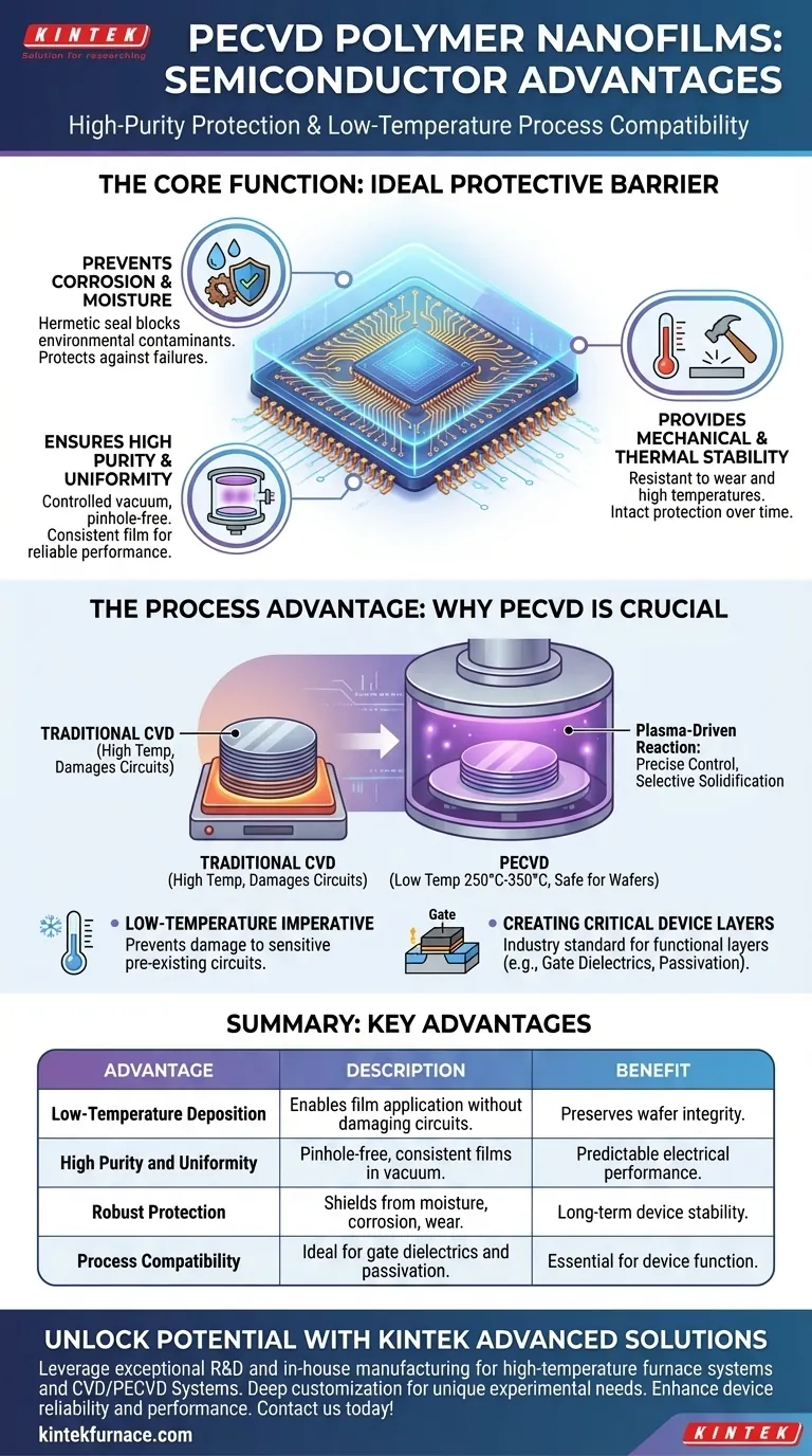
For semiconductor applications, PECVD polymer nanofilms offer a unique combination of high-purity protection and process compatibility. These films provide a uniform, pinhole-free barrier that is resistant to high temperatures, wear, and corrosion. This robust protection shields sensitive internal circuits and components from moisture and contaminants, directly enhancing the long-term stability and reliability of the final device.
The critical advantage of PECVD is not just the quality of the polymer film itself, but the low-temperature deposition process. This allows for the creation of high-performance protective layers without damaging the delicate, pre-existing circuits on a semiconductor wafer, a feat impossible with traditional high-temperature methods.
The Core Function: An Ideal Protective Barrier
PECVD films serve as a microscopic armor for the intricate world of integrated circuits. Their properties are tailored to solve the fundamental challenges of protecting highly sensitive electronic components.
Preventing Corrosion and Moisture Ingress
Modern microchips have features so small that even a microscopic amount of moisture or a single corrosive ion can cause a catastrophic failure. PECVD polymer nanofilms create a hermetic seal over the device's surface.
This uniform barrier effectively blocks environmental contaminants, which is a primary reason for their use in protecting everything from consumer electronics to critical systems in new energy vehicles.
Ensuring High Purity and Uniformity
The PECVD process occurs within a highly controlled vacuum chamber, ensuring exceptionally high film purity. Precursor gases are introduced and react in a contained plasma state, preventing airborne particles or other impurities from being trapped in the film.
This process guarantees a film of uniform thickness across the entire substrate, which is essential for predictable electrical performance and consistent device reliability.
Providing Mechanical and Thermal Stability
The resulting polymer films are not only pure but also mechanically robust. They exhibit excellent wear resistance and can withstand the high temperatures encountered during subsequent manufacturing steps and the operational life of the device.
This dual resistance ensures the protective layer remains intact, preserving the integrity and function of the semiconductor device over time.
The Process Advantage: Why PECVD is Crucial
The way a film is applied is often as important as the film's material properties. For semiconductors, the PECVD process itself is a key enabling technology.
The Low-Temperature Imperative
A semiconductor wafer undergoes hundreds of process steps before a protective layer is added. The intricate transistors and circuits already built on it are extremely sensitive to heat.
Traditional Chemical Vapor Deposition (CVD) requires very high temperatures that would destroy these underlying components. PECVD operates at much lower temperatures (typically 250°C–350°C), making it one of the only ways to deposit a high-quality film on a fully fabricated wafer without ruining it.
How Plasma-Enhanced Deposition Works
Inside the deposition chamber, an electrical field ignites the precursor gases into a plasma, a glowing sheath of energized ions and electrons.
Think of it not as "baking" a layer on, but as a controlled chemical mist that selectively solidifies onto the wafer's surface. This plasma-driven reaction is highly efficient and controllable, allowing for precise film composition and thickness.
Creating Critical Device Layers
Beyond simple protection, PECVD is a cornerstone technology for fabricating the functional parts of a transistor. It is the industry-standard method for depositing essential layers like gate dielectrics and passivation layers (e.g., silicon dioxide and silicon nitride).
These films are not just protective; they are fundamental to isolating conductive layers and enabling the device to function correctly.
Understanding the Trade-offs
While powerful, PECVD is a sophisticated process with specific considerations. Understanding its limitations provides a complete picture of its role.
Film Quality vs. Deposition Rate
As with many manufacturing processes, there is often a trade-off between speed and quality. While PECVD is highly efficient, pushing for an extremely high deposition rate can sometimes result in a film with lower density or more structural defects. Engineers must carefully balance throughput with the required film integrity.
Equipment and Precursor Complexity
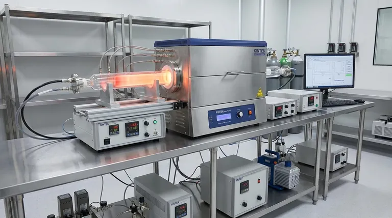
A PECVD system requires a significant investment in vacuum chambers, radio-frequency (RF) power supplies, and gas handling systems. The specialized precursor gases can also be costly. This complexity and cost are justified by the superior performance and enabling capabilities that simpler methods, like spin-coating, cannot provide.
Making the Right Choice for Your Application
Selecting the right deposition technology depends entirely on the requirements of your device and the stage of fabrication.
- If your primary focus is maximum device reliability and longevity: PECVD polymer films are the superior choice for hermetically sealing sensitive components against environmental factors like moisture and corrosion.
- If your primary focus is fabricating functional dielectric layers at low temperatures: The PECVD process is the industry standard for creating high-quality passivation or isolation films without damaging underlying chip structures.
- If your primary focus is cost-effective protection for less sensitive electronics: You might consider alternative methods like spray-on conformal coatings, but they will not offer the same level of purity, uniformity, or performance as PECVD.
Ultimately, PECVD provides an unparalleled method for depositing high-performance films at device-safe temperatures, making it an indispensable tool in modern semiconductor manufacturing.
Summary Table:
| Advantage | Description |
|---|---|
| Low-Temperature Deposition | Enables film application without damaging pre-existing circuits on wafers. |
| High Purity and Uniformity | Creates pinhole-free, consistent films in a controlled vacuum environment. |
| Robust Protection | Shields components from moisture, corrosion, and wear for long-term stability. |
| Process Compatibility | Ideal for gate dielectrics and passivation layers in semiconductor fabrication. |
Unlock the full potential of your semiconductor projects with KINTEK's advanced solutions! Leveraging exceptional R&D and in-house manufacturing, we provide diverse laboratories with high-temperature furnace systems like Muffle, Tube, Rotary, Vacuum & Atmosphere Furnaces, and CVD/PECVD Systems. Our strong deep customization capability ensures we precisely meet your unique experimental needs, enhancing device reliability and performance. Ready to elevate your research? Contact us today to discuss how we can support your innovations!
Visual Guide
Related Products
- RF PECVD System Radio Frequency Plasma Enhanced Chemical Vapor Deposition
- Slide PECVD Tube Furnace with Liquid Gasifier PECVD Machine
- Inclined Rotary Plasma Enhanced Chemical Deposition PECVD Tube Furnace Machine
- Inclined Rotary Plasma Enhanced Chemical Deposition PECVD Tube Furnace Machine
People Also Ask
- How is silicon dioxide deposited from tetraethylorthosilicate (TEOS) in PECVD? Achieve Low-Temperature, High-Quality SiO2 Films
- What are the applications of plasma enhanced chemical vapor deposition? Key Uses in Electronics, Optics & Materials
- How are deposition rates and film properties controlled in PECVD? Master Key Parameters for Optimal Thin Films
- What are the advantages of PECVD in film deposition? Achieve Low-Temp, High-Quality Coatings
- What are some promising applications of PECVD-prepared 2D materials? Unlock Advanced Sensing and Optoelectronics


